本文主要是介绍我的NPI项目之Android Camera (二) -- 核心部件之 Camera Sensor,希望对大家解决编程问题提供一定的参考价值,需要的开发者们随着小编来一起学习吧!
说到Camera模组,我们比较关心的是用的什么样的sensor? sensor的分辨率多少,sensor的像素多大,sensor是哪家生产的等等一些问题。今天,我们就穿越时间,将sensor的历史扒一扒。
Wikipedia先看一下:history of Camera
Camera的历史大体可以分为三大部分:
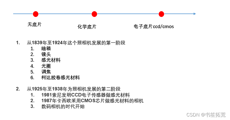
核心部件Sensor:
Sensor是什么?简单说就是传感器,用来感应什么?当然是感应光!
Sensor类型:
我所知道的sensor,有CCD的sensor,有CMOS的sensor。
What is CCD ?
CCD stands for "Charge-Coupled Device." It is a type of image sensor technology used in digital cameras and other imaging devices to capture and convert light into electronic signals.
// Charge-Copuled Device:
电荷耦合器件(charge-coupled device,CCD)是一种用于探测光的硅片,由时钟脉冲电压来产生和控制半导体势阱的变化,实现存储和传递电荷信息的固态电子器件。
A CCD image sensor is made up of an array of tiny light-sensitive elements called pixels. Each pixel is capable of converting incoming light photons into electrical charge(应该是有一种光敏材料,能够将光子转换为电子,电子汇集成电荷). The captured
charges are then transferred through the CCD chip, pixel by pixel, to a circuit where they are measured and converted into digital data that represents the image(将每个像素的电荷转化为对应的数字信号值,从而得到数值像素信息).
Here's a simplified overview of how a CCD works:
Photons of light enter the camera through the lens(镜头,后面应该还跟则滤光片Blue) and strike the surface of the CCD sensor.
The photons cause electrons in the pixels of the CCD to be excited, generating an electrical charge proportional to the intensity of the light.
The electrical charges are sequentially transferred through the CCD chip in a controlled manner, typically using a series of voltage shifts or clock signals.
The charges are read out and converted into digital values by an analog-to-digital converter (ADC) to create a digital image(模数转换后的图像信息).
CCD sensors have historically been widely used in digital cameras due to their high image quality, excellent color accuracy, and low noise performance. However, in recent years, complementary metal-oxide-semiconductor (CMOS) sensors have gained popularity due to their lower power consumption, faster readout speeds, and better integration with other circuitry on the sensor.
While CCD sensors are less common in consumer-level digital cameras today, they still find applications in specialized imaging devices, scientific cameras, medical detector, and some high-end digital cameras that prioritize image quality.
关于 CCD 到底长得什么模样以及它的组件放大图片,见下面两张:

what is CMOS ?
CMOS stands for "Complementary Metal-Oxide-Semiconductor."
互补金属氧化物半导体,作为软件出身的我,完全不懂啊,虽然数字电路/模拟电路都学过,哎。对不起,沙洲工学院的那位尽职的老师啊。
It is a type of technology used in the design and fabrication of integrated circuits, including image sensors used in digital cameras.
CMOS technology refers to the arrangement and structure of transistors and other components on a semiconductor chip. CMOS image sensors, specifically, are image sensors that utilize CMOS technology to capture and process images.
Compared to the CCD (Charge-Coupled Device) sensors, CMOS sensors have several advantages:
Lower Power Consumption: CMOS sensors typically consume less power, making them more energy-efficient.
Faster Readout Speed: CMOS sensors have faster readout speeds, allowing them to capture multiple frames per second, making them suitable for applications such as high-speed photography and video recording.
Integration with Other Circuitry: CMOS sensors can be easily integrated with other CMOS circuitry on the same chip, allowing for the integration of additional functionalities such as on-chip processing and image enhancement(ISP吗?).
Cost-Effectiveness: CMOS technology is generally more cost-effective to manufacture compared to CCD technology.
Due to these advantages, CMOS image sensors have become the dominant technology used in most consumer-level digital cameras, smartphones, webcams, and other imaging devices. They offer good image quality, flexibility, and cost-efficiency, making them suitable for a wide range of applications.
以上是对CCD和CMOS的相关理解,最根本区别会需要走到最底层半导体方面的知识了。
CCD和CMOS还有个差异是,CDD的物理像素不可个别读取,但是CMOS可以。因为,从原理上讲,CMOS 的信号是以点为单位的电荷信号,而 CCD 是以行为单位的电流信号,前者更为敏感,速度也更快,更为省电。
相关知识点:
- sensor尺寸
通常能够看到1/1.8CDD这样的描述,1/1.8是CDD sensor的尺寸。是1➗1.8✖ 1 inch为对角线的长度。 - pixel尺寸
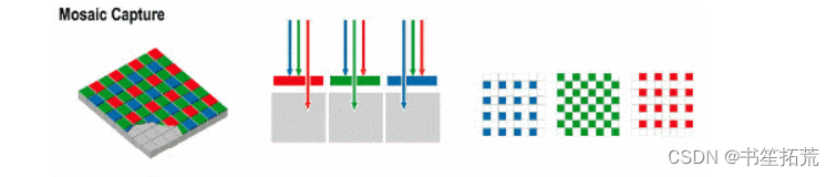
相同的像素,pixel越大感光越多,画质越好。 - Mosaic Capture 的类型
和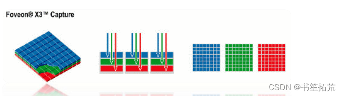
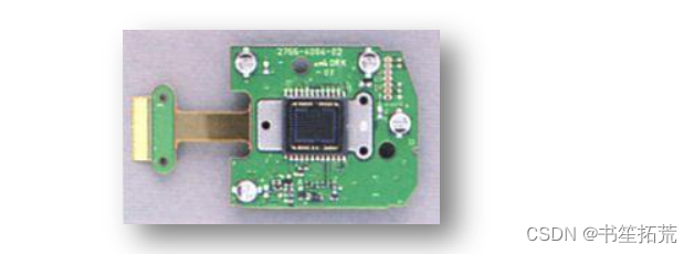
- 通常CCD芯片会和处理器(DSP/ISP)做成一个组件,类似与下图:
- 三层结构
如果切开 CCD,会发现 CCD 的结构就像三明治一样,第一层是微型镜头,第二层是分色滤色片,以及第三层感光汇流片。 - CMOS 主要 是利用硅和锗这两种元素所作成的半导体,通过 CMOS 上带负电和带正电的晶体管来实现基本的功能的。这两个互补效应所 产生的电流即可被处理芯片记录和解读成影像。
Sensor 厂家:
网上知道了一个sensor生产商的世界排名:https://us.metoree.com/categories/image-sensor/
发现原来sensor有很多种类,我的项目中是消费类的digital camera使用的场景。
Vision Sensor(Banner )/ Image Sensor(Toshiba ) / Liner Image Sensors (Toshiba )/ Machine vision (Toshiba )/ 2-D Vision Sensors(Pepperl+Fuchs) /Machine vision image sensor (Cognex 康耐视 ) / Image Sensors(Rochester ) / Image Sensor (OMNIVISION ) / Linear Images Sensors (iC-Haus) / TMR Magnetic Image Sensors (MultiDimension ) / CMOS Image sensors (ams-OSRAM AG) /
COMS image sensor 世界前十排名:
Sony 索尼
Samsung Electronics 三星
STMicroelectronics 意法半导体
GalaxyCore 格科微:首页-格科微电子(上海)有限公司
Onsemi 昂赛美
SK Hynix 海力士
SmartSens Technology: 斯特威: 思特威(上海)电子科技股份有限公司 | 专注CMOS图像传感器的创新与研发
Canon 佳能
Panasonic 松下
PixelPlus
前十里面已经有两家国产公司,加油!
这篇关于我的NPI项目之Android Camera (二) -- 核心部件之 Camera Sensor的文章就介绍到这儿,希望我们推荐的文章对编程师们有所帮助!