本文主要是介绍FPGA SDRAM接口设计(四)板级验证,希望对大家解决编程问题提供一定的参考价值,需要的开发者们随着小编来一起学习吧!
目录
一、验证方法
二、实现
1、同步FIFO模块
2、按键消抖模块
3、串口发送模块
4、SDRAM控制器模块
5、顶层模块
三、仿真及上板测试
1、仿真代码
前面已经对SDRAM原理及控制器进行了讲解,以及仿真,下边将进行板级验证。
一、验证方法
使用的是小梅哥的AC620开发板,验证是使用按键将设定的8组16位数据存储到SDRAM中,随后将SDRAM中数据存储到FIFO中,当FIFO不为空时,再将数据通过串口显示到电脑端,查看接收到的数据是否与所发的数据一致。
验证这里不再做详细的说明,供学习参考。
二、实现
主要有以下几个模块:PLL时钟倍频模块、按键消抖模块、同步FIFO模块、SDRAM控制器模块和串口发送模块。
由于SDRAM控制器采用的是100MHz时钟频率,为了同步时钟,将其他模块和其他代码都使用100MHz,有些模块使用前面博客写的,前面写的是用50MHz频率,这里需要略做修改。直接看代码:
1、同步FIFO模块
//-------------------------------------------------------------------
//https://blog.csdn.net/qq_33231534 PHF的CSDN
//File name:           syn_fifo.v
//Last modified Date:  2020/5/18
//Last Version:
//Descriptions:        Synchronize fifo 12*100(位宽*深度)
//-------------------------------------------------------------------module sync_fifo
#(parameter WIDTH         = 12,          //缓存的数据宽度parameter DEPTH         = 100,         //缓存的数据深度parameter MAX_DEPTH_BIT = 7)           //可设置的最大深度位数7,即最大深度为2^7-1
(input                                 clk         , //系统时钟50MHzinput                                 rst_n       , //系统复位input                                 wrreq       , //写使能input        [ WIDTH-1: 0]            data        , //写数据input                                 rdreq       , //读使能output  reg  [ WIDTH-1: 0]            q           , //读数据output                                empty       , //空信号output                                full        , //满信号output                                half        , //半满信号output  reg  [MAX_DEPTH_BIT-1:0]      usedw         //fifo中剩余数据个数
);reg   [ WIDTH-1: 0]     fifo_rom     [ DEPTH-1: 0]; //fifo存储单元reg   [  MAX_DEPTH_BIT-1: 0]         wr_p     ; //写指针
reg   [  MAX_DEPTH_BIT-1: 0]         rd_p     ; //读指针//当写使能且数据不满时写入数据
always  @(posedge clk )beginif(wrreq && !full) beginfifo_rom[wr_p] <= data;endelse beginfifo_rom[wr_p] <= fifo_rom[wr_p];end
end//写指针,当写使能且数据不满时,指针加一;当指针指向最大深度且有写使能时指针归零
always  @(posedge clk or negedge rst_n)beginif(rst_n==1'b0)beginwr_p <= 0;endelse if(wrreq && !full) begin if(wr_p==DEPTH-1 && wrreq)wr_p <= 0;elsewr_p <= wr_p + 1'b1;end
end//读指针,,当读使能且数据不空时,指针加一,当指针指向最大深度且有读使能时指针归零
always  @(posedge clk or negedge rst_n)beginif(rst_n==1'b0)beginrd_p <= 0;endelse if(rdreq && !empty) beginif(rd_p==DEPTH-1 && rdreq)rd_p <= 0;elserd_p <= rd_p + 1'b1;end
end//读出数据,在读使能且数据不为空时读出数据
always  @(posedge clk or negedge rst_n)beginif(rst_n==1'b0)beginq <= 0;endelse if(rdreq && !empty) beginq <= fifo_rom[rd_p];end
end//fifo中数据个数
always  @(posedge clk or negedge rst_n)beginif(rst_n==1'b0)beginusedw <= 0;endelse if((wrreq && !full && !rdreq) || (wrreq && rdreq && empty)) beginusedw <= usedw + 1'b1;endelse if(!wrreq && !empty && rdreq)beginusedw <= usedw - 1'b1;end
end//满、空、半满标志
assign full  = usedw==DEPTH;
assign empty = usedw==0;
assign half  = usedw==DEPTH/2;endmodule
2、按键消抖模块
// Company  :
// Engineer :
// -----------------------------------------------------------------------------
// https://blog.csdn.net/qq_33231534    PHF's CSDN blog
// -----------------------------------------------------------------------------
// Create Date    : 2020-09-04 15:16:47
// Revise Data    : 2020-09-04 15:17:04
// File Name      : key_filter.v
// Target Devices : XC7Z015-CLG485-2
// Tool Versions  : Vivado 2019.2
// Revision       : V1.1
// Editor         : sublime text3, tab size (4)
// Description    : 按键消抖模块module key_filter(input                   clk         ,//系统时钟100MHzinput                   rst_n       ,//系统复位input                   key_in      ,//按键输入,低为按下output   reg            key_flag    ,//输出一个脉冲按键有效信号output   reg            key_state    //输出按键状态,1为未按下,0为按下
);localparam IDLE      = 4'b0001      ;//空闲状态,读取按键按下的下降沿,读取到下降沿转到下一个状态
localparam FILTER1   = 4'b0010      ;//计数20ms状态,计数结束转到下一个状态
localparam STABLE    = 4'b0100      ;//数据稳定状态,等待按键松开上升沿,读取到上升沿转到下一个状态
localparam FILTER2   = 4'b1000      ;//计数20ms状态,计数结束转到空闲状态parameter TIME_20MS = 21'd2000_000 ;reg   [  3: 0]         state_c      ;//寄存器改变状态
reg   [  3: 0]         state_n      ;//现在状态wire                   IDLE_to_FILTER1  ;//IDLE状态转到FILTER1状态条件
wire                   FILTER1_to_STABLE;//FILTER1状态转到STABLE状态条件
wire                   STABLE_to_FILTER2;//STABLE状态转到FILTER2状态条件
wire                   FILTER2_to_IDLE  ;//FILTER2状态转到IDLE状态条件reg                    key_in_ff0   ;
reg                    key_in_ff1   ;
reg                    key_in_ff2   ;wire                   key_in_pos   ;//检测上升沿标志
wire                   key_in_neg   ;//检测下降沿标志reg   [ 20: 0]         cnt          ;
wire                   add_cnt      ;
wire                   end_cnt      ;//状态机第一段,状态转换
always  @(posedge clk or negedge rst_n)beginif(rst_n==1'b0)beginstate_c <= IDLE;endelse beginstate_c <= state_n;end
end//状态机第二段,状态转换条件
always  @(*)begincase(state_c)IDLE   :beginif(IDLE_to_FILTER1)state_n = FILTER1;elsestate_n = state_c;endFILTER1:beginif(FILTER1_to_STABLE)state_n = STABLE;elsestate_n = state_c;endSTABLE :beginif(STABLE_to_FILTER2)state_n = FILTER2;elsestate_n = state_c;endFILTER2:beginif(FILTER2_to_IDLE)state_n = IDLE;elsestate_n = state_c;enddefault:state_n = IDLE;endcase
end//状态转换条件
assign IDLE_to_FILTER1   = key_in_neg   ;
assign FILTER1_to_STABLE = state_c==FILTER1 && end_cnt;
assign STABLE_to_FILTER2 = key_in_pos   ;
assign FILTER2_to_IDLE   = state_c==FILTER2 && end_cnt;//打两拍,防止亚稳态
always  @(posedge clk or negedge rst_n)beginif(rst_n==1'b0)beginkey_in_ff0 <= 1;key_in_ff1 <= 1;key_in_ff2 <= 1;endelse beginkey_in_ff0 <= key_in;key_in_ff1 <= key_in_ff0;key_in_ff2 <= key_in_ff1;end
end//下降沿和上升沿检测
assign key_in_pos = (state_c==STABLE) ?(key_in_ff1 && !key_in_ff2):1'b0;
assign key_in_neg = (state_c==IDLE) ?(!key_in_ff1 && key_in_ff2):1'b0;//计数20ms
always @(posedge clk or negedge rst_n)beginif(!rst_n)begincnt <= 0;endelse if(add_cnt)beginif(end_cnt)cnt <= 0;elsecnt <= cnt + 1'b1;endelse begincnt <= 0;end
endassign add_cnt = state_c==FILTER1 || state_c==FILTER2;
assign end_cnt = add_cnt && cnt== TIME_20MS-1;//key_flag按键按下输出一个脉冲信号
always  @(posedge clk or negedge rst_n)beginif(rst_n==1'b0)beginkey_flag <= 0;endelse if(state_c==FILTER1 && end_cnt) beginkey_flag <= 1;endelse beginkey_flag <= 0;end
end//key_state按键按下状态信号
always  @(posedge clk or negedge rst_n)beginif(rst_n==1'b0)beginkey_state <= 1;endelse if(state_c==STABLE || state_c==FILTER2) beginkey_state <= 0;endelse beginkey_state <= 1;end
end
endmodule
3、串口发送模块
// Company  :
// Engineer :
// -----------------------------------------------------------------------------
// https://blog.csdn.net/qq_33231534    PHF's CSDN blog
// -----------------------------------------------------------------------------
// Create Date    : 2020-07-31 11:19:07
// Revise Data    : 2020-07-31 11:19:07
// File Name      : uart_tx.v
// Target Devices : XC7Z015-CLG485-2
// Tool Versions  : Vivado 2019.2
// Revision       : V1.1
// Editor         : sublime text3, tab size (4)
// Description    : uart串口发送模块,可设置波特率(4800bps/9600bps/19200bps/38400bps/57600bps/115200bps)module uart_tx(input			clk			,//100MHzinput			rst_n		,input			send_en		,input	[7:0]	send_data	,input	[2:0]	baud_set	,output	reg		tx_data		,output	reg		tx_done		,output	reg		uart_state);parameter SEND_DATA_NUM = 10; //send data numbersreg		[14:0]		baud_cnt 	;reg		[14:0]		cnt_1bit	;wire				add_cnt_1bit;wire				end_cnt_1bit;reg		[3:0]		cnt_8bit	;wire				add_cnt_8bit;wire				end_cnt_8bit;reg		[7:0]		send_data_f ;wire	[9:0]		data_out;always @(*)begincase(baud_set)3'd0:baud_cnt = 15'd20833	; //4800bps3'd1:baud_cnt = 15'd10416	; //9600bps3'd2:baud_cnt = 15'd5208 	; //19200bps3'd3:baud_cnt = 15'd2604 	; //38400bps3'd4:baud_cnt = 15'd1736 	; //57600bps3'd5:baud_cnt = 15'd868  	; //115200bpsdefault:baud_cnt = 15'd868	; //default 115200bpsendcaseendalways @(posedge clk or negedge rst_n) beginif (!rst_n) beginuart_state <= 0;		endelse if (send_en) beginuart_state <= 1;endelse if (tx_done) beginuart_state <= 0;endelse beginuart_state <= uart_state;endendalways @(posedge clk or negedge rst_n) beginif (!rst_n) begincnt_1bit <= 0;endelse if (add_cnt_1bit) beginif (end_cnt_1bit) begincnt_1bit <= 0;endelse begincnt_1bit <= cnt_1bit + 1'b1;endendelse begincnt_1bit <= 0;endendassign add_cnt_1bit = uart_state==1;assign end_cnt_1bit = add_cnt_1bit && cnt_1bit==baud_cnt-1;always @(posedge clk or negedge rst_n) beginif (!rst_n) begincnt_8bit <= 0;endelse if (add_cnt_8bit) beginif (end_cnt_8bit) begincnt_8bit <= 0;endelse begincnt_8bit <= cnt_8bit + 1'b1;endendendassign add_cnt_8bit = end_cnt_1bit;assign end_cnt_8bit = add_cnt_8bit && cnt_8bit==SEND_DATA_NUM-1;always @(posedge clk or negedge rst_n) beginif (!rst_n) beginsend_data_f <= 0;		endelse if (send_en) beginsend_data_f <= send_data;endelse beginsend_data_f <= send_data_f;endendassign data_out = {1'b1,send_data_f,1'b0};always @(posedge clk or negedge rst_n) beginif (!rst_n) begintx_data	<= 1;	endelse if (uart_state==1 && cnt_1bit==0) begintx_data <= data_out[cnt_8bit];endendalways @(posedge clk or negedge rst_n) beginif (!rst_n) begintx_done <= 0;		endelse if (uart_state==1 && end_cnt_8bit) begintx_done <= 1;endelse begintx_done <= 0;endend
endmodule
4、SDRAM控制器模块
为了文章完整性,把他放上来。
// Company  :
// Engineer :
// -----------------------------------------------------------------------------
// https://blog.csdn.net/qq_33231534    PHF's CSDN blog
// -----------------------------------------------------------------------------
// Create Date    : 2020-09-18 14:20:22
// Revise Data    : 2020-09-20 15:30:16
// File Name      : SDRAM_control.v
// Target Devices : XC7Z015-CLG485-2
// Tool Versions  : Vivado 2019.2
// Revision       : V1.1
// Editor         : sublime text3, tab size (4)
// Description    : SDRAM控制器,支持读写冲突长度为8,cas为3module SDRAM_control(input					clk				,//100MHZinput					rst_n			,//复位input					wr_en			,//写使能信号input	[15:0]			wr_data			,//写数据input					rd_en			,//读使能信号input	[1:0]			bank_addr		,//bank地址input	[11:0]			row_addr		,//行地址input	[8:0]			col_addr		,//列地址output	reg	[15:0]		rd_data			,//读出的数据output	reg				rd_data_vld		,//读出数据有效位output	wire			wr_data_vld		,//写入数据有效位output	wire			wdata_done		,//写数据结束标志output	wire			rdata_done		,//读数据结束标志output	wire			sdram_clk		,//SDRAM时钟信号output	reg	[3:0]		sdram_commond	,//{cs,ras,cas,we}output	wire			sdram_cke		,//时钟使能信号output	reg	[1:0]		sdram_dqm		,//数据线屏蔽信号output	reg	[11:0]		sdram_addr		,//SDRAM地址线output	reg	[1:0]		sdram_bank		,//SDRAM bank选取inout	wire[15:0]		sdram_dq		 //SDRAM数据输出输入总线);//延时localparam TWAIT_200us 	= 15'd20000		;//上电等待时间localparam TRP			= 2'd3			;//预充电周期localparam TRC 			= 4'd10			;//自刷新周期localparam TRSC			= 2'd3			;//加载模式寄存器周期localparam TRCD			= 2'd2			;//激活命令周期localparam TREAD_11		= 4'd11			;//burst=8,cas=3localparam TWRITE_8		= 4'd8			;//burst=8localparam AUTO_REF_TIME= 11'd1562		;//状态localparam NOP			= 3'd0			;localparam PRECHARGE	= 3'd1			;localparam REF			= 3'd2			;localparam MODE			= 3'd3			;localparam IDLE			= 3'd4			;localparam ACTIVE		= 3'd5			;localparam WRITE		= 3'd6			;localparam READ			= 3'd7			;//操作命令localparam NOP_CMD      = 4'b0111		;localparam PRECHARGE_CMD= 4'b0010		;localparam REF_CMD      = 4'b0001		;localparam MODE_CMD     = 4'b0000		;localparam ACTIVE_CMD   = 4'b0011		;localparam WRITE_CMD    = 4'b0100		;localparam READ_CMD     = 4'b0101		;//初始化阶段地址线localparam ALL_BANK		= 12'b01_0_00_000_0_000;//预充电地址线localparam MODE_CONFIG	= 12'b00_0_00_011_0_011;//配置模式寄存器时地址线wire nop_to_pre_start 		;wire pre_to_ref_start 		;wire pre_to_idle_start 		;wire ref_to_mode_start 		;wire ref_to_idle_start 		;wire ref_to_ref_start 		;wire mode_to_idle_start 	;wire idle_to_active_start 	;wire idle_to_ref_start 		;wire active_to_write_start	;wire active_to_read_start 	;wire write_to_pre_start 	;wire read_to_pre_start 		;reg	[2:0]	state_c			;reg	[2:0]	state_n			;wire 		sdram_dq_en		;wire[15:0]	sdram_dq_r		;reg			rd_data_vld_ff0	;reg			rd_data_vld_ff1	;reg			rd_data_vld_ff2	;reg			rd_data_vld_ff3	;reg	[10:0]	auto_ref_cnt	;wire		add_auto_ref_cnt;wire		end_auto_ref_cnt;reg 		ref_req			;wire 		init_done		;reg  		init_flag		;reg	[14:0]	cnt0			;wire		add_cnt0		;wire		end_cnt0		;reg [14:0]	x				;reg	[3:0]	ref_cnt1		;wire		add_cnt1		;wire		end_cnt1		;reg			flag_rd			;		reg 		flag_wr			;		assign sdram_clk = ~clk;always @(posedge clk or negedge rst_n) beginif (!rst_n) beginstate_c <= NOP;			endelse beginstate_c <= state_n;endendalways @(*)begincase(state_c)NOP	:beginif (nop_to_pre_start) beginstate_n = PRECHARGE;endelse beginstate_n = state_c;endendPRECHARGE:beginif (pre_to_ref_start) beginstate_n = REF;endelse if (pre_to_idle_start) beginstate_n = IDLE;endelse beginstate_n = state_c;endendREF:beginif (ref_to_mode_start) beginstate_n = MODE;endelse if (ref_to_idle_start) beginstate_n = IDLE;endelse if (ref_to_ref_start) beginstate_n = REF;endelse beginstate_n = state_c;endendMODE:beginif (mode_to_idle_start) beginstate_n = IDLE;endelse beginstate_n =state_c;endendIDLE:beginif (idle_to_active_start) beginstate_n = ACTIVE;endelse if (idle_to_ref_start) beginstate_n = REF;endelse beginstate_n = state_c;endendACTIVE:beginif (active_to_write_start) beginstate_n = WRITE;endelse if (active_to_read_start) beginstate_n = READ;endelse beginstate_n = state_c;endendWRITE:beginif(write_to_pre_start)beginstate_n = PRECHARGE;endelse beginstate_n = state_c;endendREAD:beginif (read_to_pre_start) beginstate_n = PRECHARGE;endelse beginstate_n = state_c;endenddefault:state_n = IDLE;endcaseendassign nop_to_pre_start 		= (state_c==NOP && end_cnt0);assign pre_to_ref_start 		= (state_c==PRECHARGE && end_cnt0 && init_flag==1);assign pre_to_idle_start 		= (state_c==PRECHARGE && end_cnt0 && init_flag==0);assign ref_to_mode_start 		= (state_c==REF && init_flag==1 && end_cnt1);assign ref_to_idle_start 		= (state_c==REF && init_flag==0 && end_cnt0);assign ref_to_ref_start 		= (state_c==REF && init_flag==1 && end_cnt0 && ref_cnt1<7);assign mode_to_idle_start 		= (state_c==MODE && init_flag==1 && end_cnt0);assign idle_to_active_start 	= (state_c==IDLE && (wr_en || rd_en) && ref_req==0);assign idle_to_ref_start 		= (state_c==IDLE && ref_req==1);assign active_to_write_start	= (state_c==ACTIVE && end_cnt0 && flag_wr);assign active_to_read_start 	= (state_c==ACTIVE && end_cnt0 && flag_rd);assign write_to_pre_start 		= (state_c==WRITE && end_cnt0);assign read_to_pre_start 		= (state_c==READ && end_cnt0);//命令控制字 sdram_commond = {CS,RAS,CAS,WE};always @(posedge clk or negedge rst_n)beginif (!rst_n) beginsdram_commond <= NOP_CMD;endelse if (nop_to_pre_start || write_to_pre_start || read_to_pre_start) beginsdram_commond <= PRECHARGE_CMD;endelse if (pre_to_ref_start || ref_to_ref_start || idle_to_ref_start) beginsdram_commond <= REF_CMD;endelse if (ref_to_mode_start) beginsdram_commond <= MODE_CMD;endelse if (idle_to_active_start) beginsdram_commond <= ACTIVE_CMD;endelse if (active_to_write_start) beginsdram_commond <= WRITE_CMD;endelse if (active_to_read_start) beginsdram_commond <= READ_CMD;endelse beginsdram_commond <= NOP_CMD;endend//cke信号保持拉高assign sdram_cke = 1;//dqm信号always  @(posedge clk or negedge rst_n)beginif(!rst_n)beginsdram_dqm <= 2'b11;endelse if(init_done)beginsdram_dqm <= 2'b00;endend//地址线always  @(posedge clk or negedge rst_n)beginif(!rst_n)beginsdram_addr <= 12'b0;endelse if(nop_to_pre_start || write_to_pre_start || read_to_pre_start)beginsdram_addr <= ALL_BANK;             endelse if(ref_to_mode_start)beginsdram_addr <= MODE_CONFIG;               endelse if(idle_to_active_start)beginsdram_addr <= row_addr;  		       		                 endelse if (active_to_read_start || active_to_write_start) beginsdram_addr <= {3'b000,col_addr};endelse beginsdram_addr <= 12'b0;               endend//sdram_bankalways  @(posedge clk or negedge rst_n)beginif(!rst_n)beginsdram_bank <= 2'b00;endelse if (idle_to_active_start || active_to_write_start || active_to_read_start) beginsdram_bank <= bank_addr;endelse beginsdram_bank <= 2'b00;endend//sdram_dqassign sdram_dq_en = (state_c==WRITE) ? 1'b1 : 1'b0;assign sdram_dq = sdram_dq_en ? sdram_dq_r : 16'hzzzz;assign sdram_dq_r = wr_data;assign wr_data_vld = state_c==WRITE;assign wdata_done = write_to_pre_start;assign rdata_done = read_to_pre_start;always @(posedge clk or negedge rst_n)beginif (!rst_n) beginrd_data <= 16'd0;endelse beginrd_data <= sdram_dq;endend// assign rd_data = state_c==READ ? sdram_dq:16'hzzzz;//读有效标志always @(posedge clk or negedge rst_n)beginif (!rst_n) beginrd_data_vld_ff0 <= 0;endelse if (active_to_read_start) beginrd_data_vld_ff0 <= 1;endelse if (state_c==READ && cnt0==TREAD_11-4) beginrd_data_vld_ff0 <= 0;endendalways @(posedge clk or negedge rst_n)beginif (!rst_n) beginrd_data_vld_ff1 <= 0;rd_data_vld_ff2 <= 0;rd_data_vld_ff3 <= 0;rd_data_vld     <= 0;endelse beginrd_data_vld_ff1 <= rd_data_vld_ff0;rd_data_vld_ff2 <= rd_data_vld_ff1;rd_data_vld_ff3 <= rd_data_vld_ff2;rd_data_vld     <= rd_data_vld_ff3;endend//刷新请求计数always @(posedge clk or negedge rst_n)beginif (!rst_n) beginauto_ref_cnt <= 0;endelse if (add_auto_ref_cnt) beginif (end_auto_ref_cnt) beginauto_ref_cnt <= 0;endelse beginauto_ref_cnt <= auto_ref_cnt + 1'b1;endendendassign add_auto_ref_cnt = init_flag==0;assign end_auto_ref_cnt = (add_auto_ref_cnt && auto_ref_cnt==AUTO_REF_TIME-1);//ref_req 刷新请求always @(posedge clk or negedge rst_n)beginif (!rst_n) beginref_req <= 0;endelse if (end_auto_ref_cnt) beginref_req <= 1;endelse if (state_c==IDLE && ref_req==1) beginref_req <= 0;endend//初始化标志assign init_done = (state_c==MODE && end_cnt0);always @(posedge clk or negedge rst_n)beginif (!rst_n) begininit_flag <= 1;endelse if (init_done) begininit_flag <= 0;endendalways @(posedge clk or negedge rst_n)beginif (!rst_n) begincnt0 <= 0;endelse if (add_cnt0) beginif (end_cnt0) begincnt0 <= 0;endelse begincnt0 <= cnt0 + 1'b1;endendendassign add_cnt0 = state_c!=IDLE;assign end_cnt0 = add_cnt0 && cnt0==x-1'b1;always @(*)begincase(state_c)NOP			: x = TWAIT_200us;PRECHARGE	: x = TRP;REF			: x = TRC;MODE		: x = TRSC;ACTIVE		: x = TRCD;WRITE		: x = TWRITE_8;READ		: x = TREAD_11;default		: x = 0;endcaseend//初始化自刷新8个周期计数always @(posedge clk or negedge rst_n)beginif (!rst_n) beginref_cnt1 <= 0;endelse if (add_cnt1) beginif (end_cnt1) beginref_cnt1 <= 0;endelse beginref_cnt1 <= ref_cnt1 + 1'b1;endendendassign add_cnt1 = (state_c==REF && init_flag==1 && end_cnt0);assign end_cnt1 = (add_cnt1 && ref_cnt1== 8-1);//读写信号标志always @(posedge clk or negedge rst_n)beginif (!rst_n) beginflag_rd <= 0;endelse if (state_c==IDLE && rd_en && ref_req==0) beginflag_rd <= 1;endelse if (pre_to_idle_start && flag_rd==1) beginflag_rd <= 0;endendalways @(posedge clk or negedge rst_n)beginif (!rst_n) beginflag_wr <= 0;endelse if (state_c==IDLE && wr_en && rd_en==0 && ref_req==0) begin  //读优先级高于写优先级flag_wr <= 1;endelse if (pre_to_idle_start && flag_wr==1) beginflag_wr <= 0;endendendmodule
5、顶层模块
// Company  :
// Engineer :
// -----------------------------------------------------------------------------
// https://blog.csdn.net/qq_33231534    PHF's CSDN blog
// -----------------------------------------------------------------------------
// Create Date    : 2020-09-23 09:29:09
// Revise Data    : 2020-09-24 09:32:26
// File Name      : SDRAM_control_test_top.v
// Target Devices : XC7Z015-CLG485-2
// Tool Versions  : Vivado 2019.2
// Revision       : V1.1
// Editor         : sublime text3, tab size (4)
// Description    :
\
module SDRAM_control_test_top(input				clk				,//50MHzinput				rst_n			,input				key_in			,output				tx_data			,output				sdram_clk		,//SDRAM时钟信号100MHzoutput	[3:0]		sdram_commond	,//{cs,ras,cas,we}output				sdram_cke		,//时钟使能信号output	[1:0]		sdram_dqm		,//数据线屏蔽信号output	[11:0]		sdram_addr		,//SDRAM地址线output	[1:0]		sdram_bank		,//SDRAM bank选取inout	[15:0]		sdram_dq		 //SDRAM数据输出输入总线);wire		key_flag	;reg			rdreq		;wire[15:0]	q			;wire		empty		;reg			send_en		;reg	[7:0]	send_data	;wire		tx_done  	;reg			wr_en		;reg	[15:0]	wr_data		;reg			rd_en		;reg	[1:0]	bank_addr	;reg	[11:0]	row_addr	;reg	[8:0]	col_addr	;wire[15:0]	rd_data		;wire		rd_data_vld	;wire		wr_data_vld	;wire		wdata_done	;wire		rdata_done	;reg			add_flag	;reg	[2:0]	cnt 		;wire		add_cnt		;wire		end_cnt		;reg			rd_fifo_flag;reg			uart_cnt	;wire		clk_100M	;pll_clk inst_pll_clk (.inclk0(clk), .c0(clk_100M));key_filter inst_key_filter (.clk       (clk_100M),.rst_n     (rst_n),.key_in    (key_in),.key_flag  (key_flag),.key_state ());sync_fifo #(.WIDTH(16),.DEPTH(24),.MAX_DEPTH_BIT(5)) inst_sync_fifo (.clk   (clk_100M),.rst_n (rst_n),.wrreq (rd_data_vld),.data  (rd_data),.rdreq (rdreq),.q     (q),.empty (empty),.full  (),.half  (),.usedw ());SDRAM_control inst_SDRAM_control(.clk           (clk_100M),.rst_n         (rst_n),.wr_en         (wr_en),.wr_data       (wr_data),.rd_en         (rd_en),.bank_addr     (bank_addr),.row_addr      (row_addr),.col_addr      (col_addr),.rd_data       (rd_data),.rd_data_vld   (rd_data_vld),.wr_data_vld   (wr_data_vld),.wdata_done    (wdata_done),.rdata_done    (rdata_done),.sdram_clk     (sdram_clk),.sdram_commond (sdram_commond),.sdram_cke     (sdram_cke),.sdram_dqm     (sdram_dqm),.sdram_addr    (sdram_addr),.sdram_bank    (sdram_bank),.sdram_dq      (sdram_dq));uart_tx inst_uart_tx(.clk        (clk_100M),.rst_n      (rst_n),.send_en    (send_en),.send_data  (send_data),.baud_set   (3'd1),.tx_data    (tx_data),.tx_done    (tx_done),.uart_state ());always @(posedge clk_100M or negedge rst_n) beginif (!rst_n) beginwr_en <= 0;endelse if (key_flag) beginwr_en <= 1;endelse beginwr_en <= 0;endendlocalparam wr_data_ini = 16'd100;always @(posedge clk_100M or negedge rst_n) beginif (!rst_n) beginwr_data <= 0;endelse if (key_flag) beginwr_data <= wr_data_ini + 4'd8;endelse if (wr_data_vld) beginwr_data <= wr_data + 1'b1;endendalways @(posedge clk_100M or negedge rst_n) beginif (!rst_n) beginbank_addr <= 2'b00;row_addr <= 12'd0;col_addr <= 9'd0;endelse if (key_flag) beginbank_addr <= 2'b00;row_addr <= row_addr + 1'b1;col_addr <= col_addr + 4'd8;endelse beginbank_addr <= bank_addr;row_addr <= row_addr;col_addr <= col_addr;endendalways @(posedge clk_100M or negedge rst_n) beginif (!rst_n) beginadd_flag <= 0;endelse if (wdata_done) beginadd_flag <= 1;endelse if (end_cnt) beginadd_flag <= 0;endendalways @(posedge clk_100M or negedge rst_n) beginif (!rst_n) begincnt <= 0;endelse if (add_cnt) beginif (end_cnt) begincnt <= 0;endelse begincnt <= cnt + 1'b1;endendendassign add_cnt = add_flag;assign end_cnt = add_cnt && cnt==5;always @(posedge clk_100M or negedge rst_n) beginif (!rst_n) beginrd_en <= 0;endelse if (end_cnt) beginrd_en <= 1;endelse beginrd_en <= 0;endendalways @(posedge clk_100M or negedge rst_n) beginif (!rst_n) beginrd_fifo_flag <= 0;endelse if (empty==0 && uart_cnt==0) beginrd_fifo_flag <= 1;endelse if (tx_done && uart_cnt==1) beginrd_fifo_flag <= 0;endendalways @(posedge clk_100M or negedge rst_n) beginif (!rst_n) beginrdreq <= 0;endelse if (empty==0&&rd_fifo_flag==0) beginrdreq <= 1;endelse beginrdreq <= 0;endendalways @(posedge clk_100M or negedge rst_n) beginif (!rst_n) beginsend_en <= 0;endelse if (rdreq || (tx_done&&uart_cnt==0)) beginsend_en <= 1;endelse beginsend_en <= 0;endendalways @(posedge clk_100M or negedge rst_n) beginif (!rst_n) beginuart_cnt <= 0;endelse if (tx_done) beginuart_cnt <= ~uart_cnt;endelse if (rdreq) beginuart_cnt <= 0;endendalways @(posedge clk_100M or negedge rst_n) beginif (!rst_n) beginsend_data <= 8'd0;endelse if (rdreq) beginsend_data <= q[15:8];endelse if(tx_done&&uart_cnt==0) beginsend_data <= q[7:0];endendendmodule
三、仿真及上板测试
1、仿真代码
`timescale 1ns/1nsmodule SDRAM_control_test_top_tb (); /* this is automatically generated */reg rst_n;reg clk;localparam clk_period = 20;// (*NOTE*) replace reset, clock, othersreg key_in;wire tx_data;wire sdram_clk;wire [3:0] sdram_commond;wire sdram_cke;wire [1:0] sdram_dqm;wire [11:0] sdram_addr;wire [1:0] sdram_bank;wire [15:0] sdram_dq;SDRAM_control_test_top inst_SDRAM_control_test_top(.clk (clk),.rst_n (rst_n),.key_in (key_in),.tx_data (tx_data),.sdram_clk (sdram_clk),.sdram_commond (sdram_commond),.sdram_cke (sdram_cke),.sdram_dqm (sdram_dqm),.sdram_addr (sdram_addr),.sdram_bank (sdram_bank),.sdram_dq (sdram_dq));sdram_model_plus #(.addr_bits(12),.data_bits(16),.col_bits(9),.mem_sizes(2*1024)) inst_sdram_model_plus (.Dq (sdram_dq),.Addr (sdram_addr),.Ba (sdram_bank),.Clk (sdram_clk),.Cke (sdram_cke),.Cs_n (sdram_commond[3]),.Ras_n (sdram_commond[2]),.Cas_n (sdram_commond[1]),.We_n (sdram_commond[0]),.Dqm (sdram_dqm),.Debug (1'b1));initial #5 clk = 1;always #(clk_period/2) clk = ~clk ;initial begin#1;rst_n = 0;key_in = 1;#(clk_period*20);rst_n = 1;#(clk_period*20);key_in = 0;#(clk_period*2500000);key_in = 1;#(clk_period*800000);$stop;endendmodule
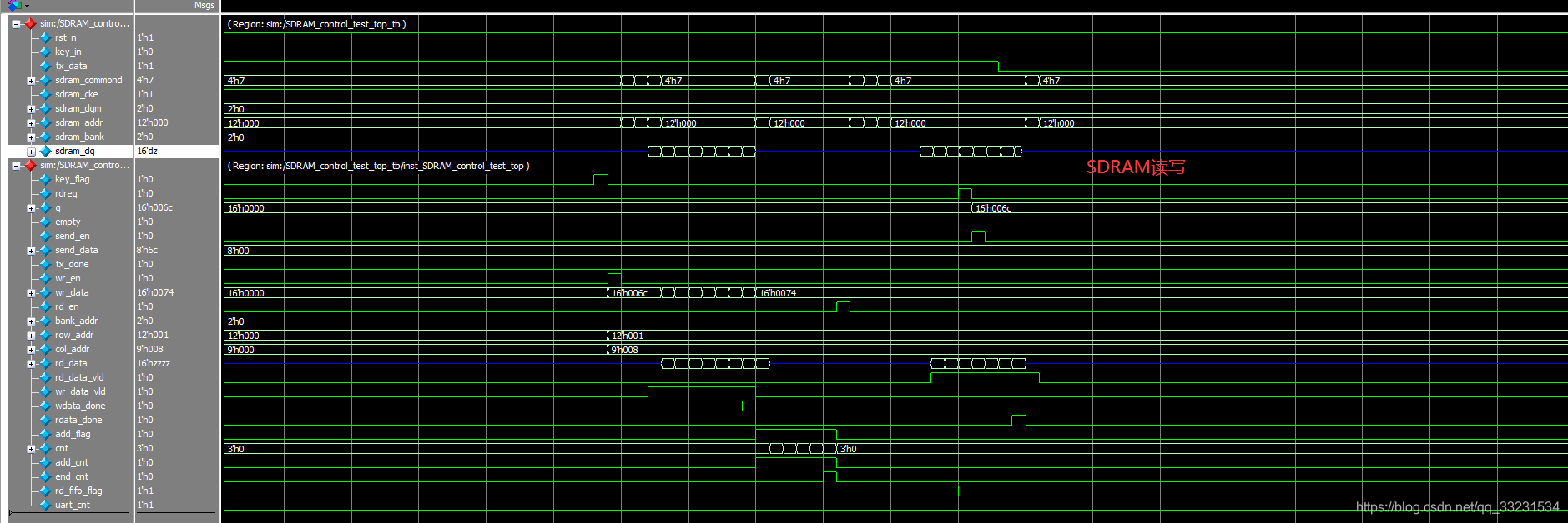
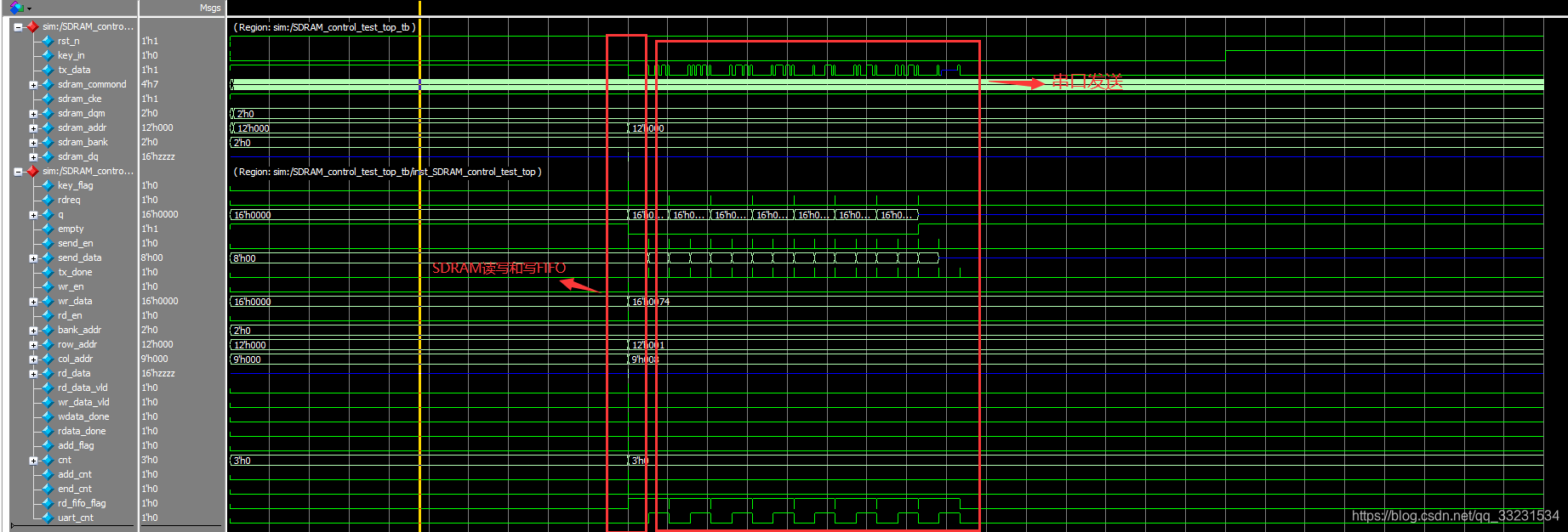
仿真图:
板子上按键按下时,串口接收数据如图:代码中发送数据为:006Ch、006Dh、006Eh、006Fh、0070h、0071h、0072h、0073h。

这篇关于FPGA SDRAM接口设计(四)板级验证的文章就介绍到这儿,希望我们推荐的文章对编程师们有所帮助!