本文主要是介绍[数字电路]用与非门实现BCD译码器驱动数码管,希望对大家解决编程问题提供一定的参考价值,需要的开发者们随着小编来一起学习吧!
Hello,大家好。这里是xdd_core,好久不见。今天来和大家聊聊大一数字电路课程的一个课设。
Key word:BCD Decoder,Proteus8.x,NAND Gate,Digital Circuit
流程:Proteus8.x仿真电路并绘制PCB导出Gerber文件打样,最终实物验证。
以下为我对这个课设的report(里面对整个设计做了详细介绍,并设计了完整的验证电路)
感谢观看,仅供参考,未经作者允许,禁止转载/抄袭,本文已上传至数据库,查重必挂QAQ
BCD to 7-Segment Decoder
Model: Digital Electronics
Table of Contents
Introduction 3
Truth table and minimum logical relationship 4
Schematic design instructions 16
Simulation method and working principle of test circuit 21
PCB layout design 27
Conclusion 29
References 30
** # Introduction**
In storage in computers, binary data is often used to represent data. However, in life, people are more accustomed to using decimal numbers to represent data. Therefore, the BCD code is generated. The BCD code uses a 4-bit binary number to represent a 0-9 decimal number. In this report, we will introduce and design a BCD code decoder composed of NAND gate and NAND gate, and use this decoder to drive a 7-segment digital tube to display digits 0-9. At the same time, a verification circuit based on the D-type flip-flop and CD4017 (decimal counter) is designed to simulate the circuit results. Finally, import the schematic diagram into a PCB file and draw a PCB drawing that complies with industry standards.
Truth table and minimum logical relationship
Before the design process below starts, the working principle of the 7-segment digital tube will be introduced first. Because this is very important for the design below.
As shown in the above figure, the 7-segment digital tube can be regarded as a combination of components arranged by 7 LEDs in a certain positional relationship on the circuit. The 7-segment digital tube is also divided into two types: common yin and common yang. Common cathode means that the cathodes (negative poles) of all LEDs are connected in parallel and led to a port (the port is denoted as COM-). If you need to light a certain segment of the ag tube, you only need to add a positive on the corresponding ag port Voltage (high level), and connect the COM- port to the negative pole of the power supply. On the contrary, the common anode means that the anodes (positive poles) of all LEDs are connected in parallel to a port (port is denoted as COM +). If you need to light up a certain segment of ag digital tube, you only need to connect the corresponding ag port to the negative pole , And connect the COM + port to the positive pole of the power supply.
In order to make it easier to use Karnaugh map to simplify the logic algebraic expressions of a-g ports later, the common cathode digital tube is selected for design in this report. Because the on and off of each segment of the common negative digital tube can be easily expressed by 1 (on) and 0 (off), which is the same as the simplification logic of the Karnaugh diagram simplified logic relationship.
As shown in the above figure, it is a schematic diagram of the entire design. The final proteus schematic diagram is more complicated than the above picture. It can be seen from the above figure that the BCD decoder circuit mainly has four inputs of A, B, C, and D, and seven outputs of a, b, c, d, e, f, and g. Here, A is the input MSB (Most Significant Bit) and D is the input LSB (least significant bit).
In propositional logic and boolean algebra, De Morgan's laws[1][2][3] are a pair of transformation rules that are both valid rules of inference. They are named after Augustus De Morgan, a 19th-century British mathematician. The rules allow the expression of conjunctions and disjunctions purely in terms of each other via negation. (Wikipedia,2020)
Since De Morgan's law (inversion law) will be used in the process of changing the logical relationship, the relevant details of this law are introduced here:
This law can easily convert the minimum logic relationship corresponding to each output of the BCD decoder into the form expressed by NAND gate and NOR gate.
The truth table corresponding to the a-g sections will be listed below in order. For convenience, the DEC column is added to the truth table to indicate the decimal number representation corresponding to the 4-bit binary number. Among them, 1 means that the corresponding segment of the nixie tube is on, 0 means that the corresponding segment of the nixie tube is off, and X is a logically unrelated item.
a segment :
From the truth table above, the Karnaugh map is:
Circle the logical adjacent items and geometric adjacent items corresponding to the Karnaugh map in different colors as follows:
In the end, the minimum logical relationship of the a segment digital tube is:
Because NAND gates and NAND gates are required for circuit design, de Morgan's law (inversion law) is used to simplify the above minimum logical relationship:
b segment:
[外链图片转存失败,源站可能有防盗链机制,建议将图片保存下来直接上传(img-ULMoLqxQ-1596257066537)(https://i.loli.net/2020/08/01/lVBhSUTcHkONxM4.png)]
From the truth table above, the Karnaugh map is:
Circle the logical adjacent items and geometric adjacent items corresponding to the Karnaugh map in different colors as follows:
[外链图片转存失败,源站可能有防盗链机制,建议将图片保存下来直接上传(img-FiWsrtHW-1596257066538)(https://i.loli.net/2020/08/01/IdjQWTcvNHrobiF.png)]
Finally, the minimum logical relationship of the b-segment digital tube is:
Because NAND gates and NAND gates are required for circuit design, de Morgan's law (inversion law) is used to simplify the above minimum logical relationship:
c segment:
From the truth table above, the Karnaugh map is:
Circle the logical adjacent items and geometric adjacent items corresponding to the Karnaugh map in different colors as follows:
In the end, the minimum logical relationship of the c-segment digital tube is:
Because NAND gates and NAND gates are required for circuit design, de Morgan's law (inversion law) is used to simplify the above minimum logical relationship:
d segment:
[外链图片转存失败,源站可能有防盗链机制,建议将图片保存下来直接上传(img-8uZGTIet-1596257066540)(https://i.loli.net/2020/08/01/uf3Rs7gNkGyVJX8.png)]
From the truth table above, the Karnaugh map is:
Circle the logical adjacent items and geometric adjacent items corresponding to the Karnaugh map in different colors as follows:
[外链图片转存失败,源站可能有防盗链机制,建议将图片保存下来直接上传(img-kzWWndTk-1596257066541)(https://i.loli.net/2020/08/01/v5WogBD6TRcALJZ.png)]
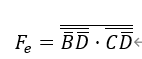
In the end, the minimum logical relationship of the d-segment digital tube is:
Because NAND gates and NAND gates are required for circuit design, de Morgan's law (inversion law) is used to simplify the above minimum logical relationship:
e segment:
[外链图片转存失败,源站可能有防盗链机制,建议将图片保存下来直接上传(img-6HipDIMp-1596257066541)(https://i.loli.net/2020/08/01/tX6UlCj1QNaci9k.png)]
From the truth table above, the Karnaugh map is:
Circle the logical adjacent items and geometric adjacent items corresponding to the Karnaugh map in different colors as follows:
Finally, the minimum logical relationship of the e-segment digital tube is:
Because NAND gates and NAND gates are required for circuit design, de Morgan's law (inversion law) is used to simplify the above minimum logical relationship:
f segment:
From the truth table above, the Karnaugh map is:
Circle the logical adjacent items and geometric adjacent items corresponding to the Karnaugh map in different colors as follows:
![[外链图片转存失败,源站可能有防盗链机制,建议将图片保存下来直接上传(img-MeSpuUbP-1596257066544)(https://i.loli.net/2020/08/01/IHik9mAacnsQqe7.png)]](https://img-blog.csdnimg.cn/20200801124530448.png?x-oss-process=image/watermark,type_ZmFuZ3poZW5naGVpdGk,shadow_10,text_aHR0cHM6Ly9ibG9nLmNzZG4ubmV0L3FxXzM2MjI5ODc2,size_16,color_FFFFFF,t_70)
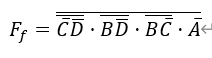
Finally, the minimum logical relationship of f segment digital tube is:
Because NAND gates and NAND gates are required for circuit design, de Morgan's law (inversion law) is used to simplify the above minimum logical relationship:
g segment:
![[外链图片转存失败,源站可能有防盗链机制,建议将图片保存下来直接上传(img-2EEUyQ9j-1596257066544)(RackMultipart20200801-4-gt2lnn_html_70d51e91e6789598.png)]](https://img-blog.csdnimg.cn/2020080112454470.png?x-oss-process=image/watermark,type_ZmFuZ3poZW5naGVpdGk,shadow_10,text_aHR0cHM6Ly9ibG9nLmNzZG4ubmV0L3FxXzM2MjI5ODc2,size_16,color_FFFFFF,t_70)
From the truth table above, the Karnaugh map is:
![[外链图片转存失败,源站可能有防盗链机制,建议将图片保存下来直接上传(img-w8BZRLAf-1596257066545)(RackMultipart20200801-4-gt2lnn_html_4d41c91ca1ae4ef4.png)]](https://img-blog.csdnimg.cn/20200801124551982.png)
Circle the logical adjacent items and geometric adjacent items corresponding to the Karnaugh map in different colors as follows:
![[外链图片转存失败,源站可能有防盗链机制,建议将图片保存下来直接上传(img-blSAm99b-1596257066545)(RackMultipart20200801-4-gt2lnn_html_8947e5872a64a3f.jpg)]](https://img-blog.csdnimg.cn/2020080112460267.png?x-oss-process=image/watermark,type_ZmFuZ3poZW5naGVpdGk,shadow_10,text_aHR0cHM6Ly9ibG9nLmNzZG4ubmV0L3FxXzM2MjI5ODc2,size_16,color_FFFFFF,t_70)
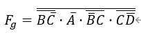
Finally, the minimum logical relationship of the g-segment digital tube is:
Because NAND gates and NAND gates are required for circuit design, de Morgan's law (inversion law) is used to simplify the above minimum logical relationship:
Schematic design instructions
![[外链图片转存失败,源站可能有防盗链机制,建议将图片保存下来直接上传(img-4DxQwJDP-1596257066545)(RackMultipart20200801-4-gt2lnn_html_462b177c6f649379.png)]](https://img-blog.csdnimg.cn/20200801124613296.png?x-oss-process=image/watermark,type_ZmFuZ3poZW5naGVpdGk,shadow_10,text_aHR0cHM6Ly9ibG9nLmNzZG4ubmV0L3FxXzM2MjI5ODc2,size_16,color_FFFFFF,t_70)
In order to make the whole schematic diagram more concise, clear and tidy. The above schematic diagram uses the proteus network label to merge the same network, which greatly reduces the number of wiring. The whole schematic diagram is divided into 4 parts, the first part is the BCD decoder implemented with NAND gate and NAND gate, the second part is the digital tube display part, and the third part is the verification circuit part (for verification Whether other circuits work normally), the fourth part is the input terminal part. The sections 1, 2, and 4 will be introduced one by one. Part 3 will be introduced in the next chapter.
Part 1: BCD decoder circuit
Deduced from the above minimum logical relationship, the minimum logical relationship of segment a of the digital tube is:
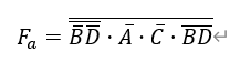
Therefore, the schematic diagram drawn in proteus according to the above logical relationship is:
![[外链图片转存失败,源站可能有防盗链机制,建议将图片保存下来直接上传(img-RouDrEZY-1596257066547)(RackMultipart20200801-4-gt2lnn_html_67ac942866f63636.png)]](https://img-blog.csdnimg.cn/20200801124625858.png?x-oss-process=image/watermark,type_ZmFuZ3poZW5naGVpdGk,shadow_10,text_aHR0cHM6Ly9ibG9nLmNzZG4ubmV0L3FxXzM2MjI5ODc2,size_16,color_FFFFFF,t_70)
Deduced from the above minimum logical relationship, the minimum logical relationship of segment b of the digital tube is:
Therefore, the schematic diagram drawn in proteus according to the above logical relationship is:
![[外链图片转存失败,源站可能有防盗链机制,建议将图片保存下来直接上传(img-PKlCSrXo-1596257066547)(RackMultipart20200801-4-gt2lnn_html_a61513400cb5a31c.png)]](https://img-blog.csdnimg.cn/20200801124637838.png?x-oss-process=image/watermark,type_ZmFuZ3poZW5naGVpdGk,shadow_10,text_aHR0cHM6Ly9ibG9nLmNzZG4ubmV0L3FxXzM2MjI5ODc2,size_16,color_FFFFFF,t_70)
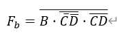
Deduced from the above minimum logical relationship, the minimum logical relationship of segment c of the digital tube is:

Therefore, the schematic diagram drawn in proteus according to the above logical relationship is:
![[外链图片转存失败,源站可能有防盗链机制,建议将图片保存下来直接上传(img-lg7BOImq-1596257066547)(RackMultipart20200801-4-gt2lnn_html_7e4bfe96de7673da.png)]](https://img-blog.csdnimg.cn/20200801124749254.png?x-oss-process=image/watermark,type_ZmFuZ3poZW5naGVpdGk,shadow_10,text_aHR0cHM6Ly9ibG9nLmNzZG4ubmV0L3FxXzM2MjI5ODc2,size_16,color_FFFFFF,t_70)
Deduced from the above minimum logical relationship, the minimum logical relationship of the d segment of the digital tube is:
Therefore, the schematic diagram drawn in proteus according to the above logical relationship is:
![[外链图片转存失败,源站可能有防盗链机制,建议将图片保存下来直接上传(img-nVxKl9yJ-1596257066548)(RackMultipart20200801-4-gt2lnn_html_2eaf121bf51f0fab.png)]](https://img-blog.csdnimg.cn/20200801124807298.png?x-oss-process=image/watermark,type_ZmFuZ3poZW5naGVpdGk,shadow_10,text_aHR0cHM6Ly9ibG9nLmNzZG4ubmV0L3FxXzM2MjI5ODc2,size_16,color_FFFFFF,t_70)
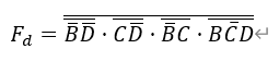
Deduced from the above minimum logical relationship, the minimum logical relationship of the digital tube e segment is:
Therefore, the schematic diagram drawn in proteus according to the above logical relationship is:
![[外链图片转存失败,源站可能有防盗链机制,建议将图片保存下来直接上传(img-zneoYFCy-1596257066548)(RackMultipart20200801-4-gt2lnn_html_76ce5165c38fc42c.png)]](https://img-blog.csdnimg.cn/20200801124827347.png?x-oss-process=image/watermark,type_ZmFuZ3poZW5naGVpdGk,shadow_10,text_aHR0cHM6Ly9ibG9nLmNzZG4ubmV0L3FxXzM2MjI5ODc2,size_16,color_FFFFFF,t_70)
Derived from the above minimum logical relationship, the minimum logical relationship of the f segment of the digital tube is:
Therefore, the schematic diagram drawn in proteus according to the above logical relationship is:
![[外链图片转存失败,源站可能有防盗链机制,建议将图片保存下来直接上传(img-vwB3fVLb-1596257066549)(RackMultipart20200801-4-gt2lnn_html_6e1557f8bb6398cc.png)]](https://img-blog.csdnimg.cn/2020080112484945.png?x-oss-process=image/watermark,type_ZmFuZ3poZW5naGVpdGk,shadow_10,text_aHR0cHM6Ly9ibG9nLmNzZG4ubmV0L3FxXzM2MjI5ODc2,size_16,color_FFFFFF,t_70)
Deduced from the above minimum logical relationship, the minimum logical relationship of the g segment of the digital tube is:
Therefore, the schematic diagram drawn in proteus according to the above logical relationship is:
![[外链图片转存失败,源站可能有防盗链机制,建议将图片保存下来直接上传(img-XVH2J1lA-1596257066549)(RackMultipart20200801-4-gt2lnn_html_18118a926c60dd33.png)]](https://img-blog.csdnimg.cn/20200801124907153.png?x-oss-process=image/watermark,type_ZmFuZ3poZW5naGVpdGk,shadow_10,text_aHR0cHM6Ly9ibG9nLmNzZG4ubmV0L3FxXzM2MjI5ODc2,size_16,color_FFFFFF,t_70)
Part 2: Digital display circuit
![[外链图片转存失败,源站可能有防盗链机制,建议将图片保存下来直接上传(img-2Am6L4OF-1596257066550)(RackMultipart20200801-4-gt2lnn_html_526c3fae55e4e4c7.png)]](https://img-blog.csdnimg.cn/20200801124915516.png?x-oss-process=image/watermark,type_ZmFuZ3poZW5naGVpdGk,shadow_10,text_aHR0cHM6Ly9ibG9nLmNzZG4ubmV0L3FxXzM2MjI5ODc2,size_16,color_FFFFFF,t_70)
From the above introduction, we can know that the 7-segment digital tube integrates 7 LED lamp beads, the driving current of each LED lamp bead is 5-8ma, so a 1k resistor is connected in series with the input port of the digital tube ag (Vcc) is 5V, so it can be calculated that the current flowing through each LED lamp bead is 5ma, which meets the requirements of LED lamp bead driving. The resistor will act as a voltage divider and limit current to prevent the LED lamp bead from being burned due to high current.
The digital tube in the above picture is an 8-segment digital tube. Compared with the 7-segment digital tube, there is one more field for controlling the decimal point. In this report, the logic control of the decimal point is not involved, so in the schematic diagram, the field that controls the decimal point is connected to the power ground to ensure that it is always off.
Part 4: Input terminal circuit
![[外链图片转存失败,源站可能有防盗链机制,建议将图片保存下来直接上传(img-yL3WYIOF-1596257066550)(RackMultipart20200801-4-gt2lnn_html_55b6c23cd50d2d9.png)]](https://img-blog.csdnimg.cn/20200801124923988.png?x-oss-process=image/watermark,type_ZmFuZ3poZW5naGVpdGk,shadow_10,text_aHR0cHM6Ly9ibG9nLmNzZG4ubmV0L3FxXzM2MjI5ODc2,size_16,color_FFFFFF,t_70)
Because in the PCB design of the schematic diagram drawn in this report, in order to finally design the PCB, it can normally obtain external A, B, C, D signals, and obtain the power supply voltage for the circuit to work. Therefore, the input terminal circuit is designed as above, which is used to obtain the input of external A, B, C, D signals, and to provide the power supply voltage for the circuit operation.
Simulation method and working principle of test circuit
By analyzing the working principle of the entire schematic, we can know that the key point of the simulation test is the simulation of the four input signals A, B, C, and D. Through the previous BCD decoder truth table, you can know that the four signals of A (MSB), B, C, and D (LSB) represent 4 binary numbers, and the data range is from 0000 (DEC: 0) to 1111 (DEC : 15) One by one jump. But through the truth table, you can know that 1010 (DEC: 10) ~ 1111 (DEC: 15) is invalid (because a digital tube can only display the numbers 0 ~ 9).
Through the above requirement analysis, we can now summarize the requirements of the test circuit. 1. The test circuit should output four signals, A, B, C, and D, and make the signal change from 0000 (DEC: 0) to 1001 (DEC: 9). 2. The rate of change of the four signals A, B, C, and D should be controllable to prevent the simulation phenomenon from being difficult to observe because the signal changes too fast.
In response to the above two-point test circuit requirements, I designed the following test circuit for the simulation of the entire circuit.
![[外链图片转存失败,源站可能有防盗链机制,建议将图片保存下来直接上传(img-Yl8754vu-1596257066551)(RackMultipart20200801-4-gt2lnn_html_55ff7d933acc8df3.png)]](https://img-blog.csdnimg.cn/20200801124935947.png?x-oss-process=image/watermark,type_ZmFuZ3poZW5naGVpdGk,shadow_10,text_aHR0cHM6Ly9ibG9nLmNzZG4ubmV0L3FxXzM2MjI5ODc2,size_16,color_FFFFFF,t_70)
The test circuit is very simple to use, just add a clock excitation signal to the CLK port of U14: A, and the four input signals of A, B, C, and D can be realized from 0000 (DEC: 0) to 1001 (DEC : 9) Make changes one by one. Input the changed signal into a-g NAND gate circuit, and then the digital tube can be driven to realize the digital display of 0-9 one by one. The frequency of the signal change is determined by the frequency of the clock excitation signal of the CLK port of U14: A. For the convenience of observation, the frequency of the square wave signal is set to 1 Hz below.
![[外链图片转存失败,源站可能有防盗链机制,建议将图片保存下来直接上传(img-zBVNxyCc-1596257066551)(RackMultipart20200801-4-gt2lnn_html_9cc516e645803ea4.png)]](https://img-blog.csdnimg.cn/20200801124945442.png?x-oss-process=image/watermark,type_ZmFuZ3poZW5naGVpdGk,shadow_10,text_aHR0cHM6Ly9ibG9nLmNzZG4ubmV0L3FxXzM2MjI5ODc2,size_16,color_FFFFFF,t_70)
The test circuit consists of 4 D-type flip-flops and 2 CD4017 decimal counters, and a NOT gate. The Q port of each D-type flip-flop is connected to D (LSB), C, B, and A (MSB).
When no clock signal is received at the CLK port of U14: A, the Q ports of the four D-type flip-flops all output a 0 (low level) signal.
When the CLK port of U14: A receives a clock signal, it will output a 1 (high level) signal at Q, and the other flip-flop Q output port outputs a 0 (low level) signal, forming 0 (A) 0 ( B) 0 © 1 (D).
When the CLK port of U14: A receives the second clock signal again, the Q port of U14: A will output 0 (low level), the Q port of U14: B will output 1 (high level), and others Trigger Q output port outputs a 0 (low level) signal, forming 0 (A) 0 (B) 1 © 0 (D).
When the CLK port of U14: A receives the third clock signal again, the Q port of U14: A will output 1 (high level), the Q port of U14: B will output 1 (high level), and others The flip-flop Q output port outputs a 0 (low level) signal, forming 0 (A) 0 (B) 1 © 1 (D).
By analogy, the change of A, B, C, D from 0000 to 1111 can be achieved. Since the frequency of the input clock signal is 1 Hz, the signal jumps once every 1 second.
But through the above analysis of the test circuit requirements, we can know that the change range of the four signals A, B, C, D can not include 1010 (DEC: 10) ~ 1111 (DEC: 15). Therefore, two CD4017s are needed to limit the output signal range.
![[外链图片转存失败,源站可能有防盗链机制,建议将图片保存下来直接上传(img-p5aGhJt3-1596257066551)(RackMultipart20200801-4-gt2lnn_html_a74350ae256e88c3.png)]](https://img-blog.csdnimg.cn/20200801124959722.png?x-oss-process=image/watermark,type_ZmFuZ3poZW5naGVpdGk,shadow_10,text_aHR0cHM6Ly9ibG9nLmNzZG4ubmV0L3FxXzM2MjI5ODc2,size_16,color_FFFFFF,t_70)
CD4017 port timing diagram
The CLK port of U16 and the CLK port of U14: A are connected in parallel, so that the CD4017 can simultaneously count the input clock signal. According to the above CD4017 port timing diagram, when the CD4017 CLK port does not receive a clock signal, the Q0 port clock is high, when a clock signal is received, the Q1 port becomes high, and the other ports are Low level. By analogy, the decimal counting function of the input clock signal is realized.
For this test circuit, because the valid range of the data is 0000-1001, when the D-type flip-flop U14: A receives the tenth pulse, it is necessary to reset four D-type flip-flops (that is, the output signal Q is set zero). How to achieve this function?
First, connect the Q9 port of U16 to the CLK port of U17, and connect the Q1 port of U17 to its own reset port MR and the reset ports of four D-type flip-flops through an inverter. Since the reset port of the D-type flip-flop is active low and the CD4017 outputs a high-level signal, the role of the inverter here is to invert the level signal, so that the CD4017 can trigger the reset of the D-type flip-flop.
When the simulation starts, U9 receives 9 clock signals, and Q9 outputs a high level. When U16 receives the 10th clock signal, the state of the Q9 port of U16 changes from high level to low level, thereby generating a clock signal and inputting it to the CLK port of U17. At this time, the Q1 port of U17 outputs a high level. This high-level signal will act on the reset port MR of U17 and the reset ports of four D-type flip-flops. The effect is: 1. U17 reset (Q0 is high level, the rest is low level). 2.4 D-type flip-flop reset (all Q ports output low level, ABCD = 0000).
Through the above circuit design, the function of limiting the four signal changes of ABCD to 0000-1001 can be realized. So far, all the requirements of the test circuit have been well solved. Next you can simulate.
Simulation results:
![[外链图片转存失败,源站可能有防盗链机制,建议将图片保存下来直接上传(img-ETcQ77U7-1596257066552)(RackMultipart20200801-4-gt2lnn_html_1cf1d728411d1713.png)]](https://img-blog.csdnimg.cn/20200801125014265.png)
![[外链图片转存失败,源站可能有防盗链机制,建议将图片保存下来直接上传(img-5vL0wG1b-1596257066552)(RackMultipart20200801-4-gt2lnn_html_85952e9d781cf780.png)]](https://img-blog.csdnimg.cn/20200801125024519.png)
![[外链图片转存失败,源站可能有防盗链机制,建议将图片保存下来直接上传(img-ZfuKDU8H-1596257066553)(RackMultipart20200801-4-gt2lnn_html_b253eaf9235f056b.png)]](https://img-blog.csdnimg.cn/20200801125034864.png)
PCB layout design
![[外链图片转存失败,源站可能有防盗链机制,建议将图片保存下来直接上传(img-oOWLZDOy-1596257066557)(RackMultipart20200801-4-gt2lnn_html_92084fc5826754c1.png)]](https://img-blog.csdnimg.cn/20200801125048317.png?x-oss-process=image/watermark,type_ZmFuZ3poZW5naGVpdGk,shadow_10,text_aHR0cHM6Ly9ibG9nLmNzZG4ubmV0L3FxXzM2MjI5ODc2,size_16,color_FFFFFF,t_70)
![[外链图片转存失败,源站可能有防盗链机制,建议将图片保存下来直接上传(img-1dntVusm-1596257066557)(RackMultipart20200801-4-gt2lnn_html_66492d9edb2df0fc.jpg)]](https://img-blog.csdnimg.cn/20200801125055847.png)
![[外链图片转存失败,源站可能有防盗链机制,建议将图片保存下来直接上传(img-TfLGF43u-1596257066558)(RackMultipart20200801-4-gt2lnn_html_2b7c78962895f77c.jpg)]](https://img-blog.csdnimg.cn/20200801125103683.png)
As shown in the figure above is the layout design and 3D view of the PCB. In the above PCB layout, I followed the following design specifications:
- There is no interference between components, which greatly facilitates the assembly and welding of physical circuits.2. The power line and signal line use different line widths. The width of the power line is 25mil and the signal line is 10mil, which greatly improves the stability of the circuit and prevents the heating of the wiring caused by the large current.3. The corners of the PCB outer frame are designed with rounded corners to prevent harm to users caused by right-angled corners.4. The layout between the components is compact and there is no large free area. Thereby reducing the area of each circuit board, thereby greatly reducing production costs.5. 45 ° wiring, to avoid signal reflection caused by impedance mismatch caused by right-angle wiring or acute-angle wiring.6. The silk screen of the component and the silk screen of the input signal are clearly marked, which is convenient for welding and debugging.7. The minimum line width is greater than the process limit of 6mil, and the minimum line spacing is greater than 5mil.
PCB finished product:
![[外链图片转存失败,源站可能有防盗链机制,建议将图片保存下来直接上传(img-vy1huEOU-1596257066558)(RackMultipart20200801-4-gt2lnn_html_c093fb45fc1f00a5.jpg)]](https://img-blog.csdnimg.cn/20200801125116789.png?x-oss-process=image/watermark,type_ZmFuZ3poZW5naGVpdGk,shadow_10,text_aHR0cHM6Ly9ibG9nLmNzZG4ubmV0L3FxXzM2MjI5ODc2,size_16,color_FFFFFF,t_70)
BCD Decoder
![[外链图片转存失败,源站可能有防盗链机制,建议将图片保存下来直接上传(img-TR9j2sUq-1596257066559)(RackMultipart20200801-4-gt2lnn_html_2c514b039a752c1f.gif)]](https://img-blog.csdnimg.cn/20200801125125730.png?x-oss-process=image/watermark,type_ZmFuZ3poZW5naGVpdGk,shadow_10,text_aHR0cHM6Ly9ibG9nLmNzZG4ubmV0L3FxXzM2MjI5ODc2,size_16,color_FFFFFF,t_70)
Verification Circuit
![[外链图片转存失败,源站可能有防盗链机制,建议将图片保存下来直接上传(img-J2kkcaop-1596257066560)(RackMultipart20200801-4-gt2lnn_html_88cb8717c6bc89f2.jpg)]](https://img-blog.csdnimg.cn/20200801125137513.png?x-oss-process=image/watermark,type_ZmFuZ3poZW5naGVpdGk,shadow_10,text_aHR0cHM6Ly9ibG9nLmNzZG4ubmV0L3FxXzM2MjI5ODc2,size_16,color_FFFFFF,t_70)
The assembled circuit. (The BCD decoder circuit on the left and the verification circuit on the right)
![[外链图片转存失败,源站可能有防盗链机制,建议将图片保存下来直接上传(img-bgULCrTr-1596257066560)(RackMultipart20200801-4-gt2lnn_html_bbe092743a88c58f.jpg)]](https://img-blog.csdnimg.cn/20200801125146531.png?x-oss-process=image/watermark,type_ZmFuZ3poZW5naGVpdGk,shadow_10,text_aHR0cHM6Ly9ibG9nLmNzZG4ubmV0L3FxXzM2MjI5ODc2,size_16,color_FFFFFF,t_70)
( Running Result ,display "3")
![[外链图片转存失败,源站可能有防盗链机制,建议将图片保存下来直接上传(img-sASY44RQ-1596257066560)(RackMultipart20200801-4-gt2lnn_html_ec704b3725ca3939.jpg)]](https://img-blog.csdnimg.cn/20200801125202851.png?x-oss-process=image/watermark,type_ZmFuZ3poZW5naGVpdGk,shadow_10,text_aHR0cHM6Ly9ibG9nLmNzZG4ubmV0L3FxXzM2MjI5ODc2,size_16,color_FFFFFF,t_70)
( Running Result ,display "1")
![[外链图片转存失败,源站可能有防盗链机制,建议将图片保存下来直接上传(img-zNk2csUf-1596257066560)(RackMultipart20200801-4-gt2lnn_html_591d947ef5f71c86.jpg)]](https://img-blog.csdnimg.cn/20200801125212989.png?x-oss-process=image/watermark,type_ZmFuZ3poZW5naGVpdGk,shadow_10,text_aHR0cHM6Ly9ibG9nLmNzZG4ubmV0L3FxXzM2MjI5ODc2,size_16,color_FFFFFF,t_70)
( Running Result ,display "0")
# Conclusion
In this report, we designed and introduced a 7-segment digital tube drive circuit based on NAND gate and NAND gate, and designed the corresponding test circuit. Finally, in compliance with the PCB design specifications, all the To complete the PCB layout design. After the production, I found that the circuit in the article has the following improvements: 1. Increase the filter capacitor on the chip power supply to improve the stability of the circuit. 2. A fuse and three-terminal voltage regulator are added to the power input port to prevent the external large current or high voltage from burning the circuit. 3. PCB laying ground copper to improve anti-interference ability.
# References
**[1]wikipedia. RS-232 [EB/OL].**https://en.wikipedia.org/wiki/RS-232,2020-4-13.
23/ 23
Date:12/04/2020
感谢观看,仅供参考,未经作者允许,禁止转载/抄袭,本文已上传至数据库,查重必挂QAQ
这篇关于[数字电路]用与非门实现BCD译码器驱动数码管的文章就介绍到这儿,希望我们推荐的文章对编程师们有所帮助!