本文主要是介绍Integrated Microfluidic Cooling for S-Band 10-Watt CW Power Amplifiers on Hybrid PCBs,希望对大家解决编程问题提供一定的参考价值,需要的开发者们随着小编来一起学习吧!
Integrated Microfluidic Cooling for S-Band 10-Watt CW Power Amplifiers on Hybrid PCBs
Abstract
本文提出了一种在Rogers和FR4混合印刷电路板(PCB)上的集成微流控通道,用于在塑料表面贴装封装中冷却S波段10W连续波功率放大器。
设计并制造了一种四层混合PCB,其制造工艺完全基于标准多层PCB技术。
热和射频实验结果表明,多层混合电路板上的集成微流控冷却方案是有效的。在水流量为325ml/min时,功率放大器的外壳温度降至44℃,而在2.1 GHz时,功率增加效率(PAE)为42.6%,连续波输出功率为41.2 dBm。在比较实验中,使用传统冷却方法,功率放大器在PCB上输出相同的连续波功率,但在数十秒内失败。
外壳温度在大约10秒内迅速上升并逐渐趋于稳定。随着冷却剂流速的增加,稳态外壳温度降低。例如,流速为 7.3 mL/min 时的稳态壳体温度为 77.3 °C,流速为 84 mL/min 时为 55.7 °C。然而,当流速增加超过 220 mL/min 时,传热性能的提高是有限的。例如,当流速分别设置为 325 mL/min 和 280 mL/min 时,它们的稳态外壳温度差异仅为 0.8 °C。根据功率放大器的产品数据表,塑料封装从结到外壳的热阻为 3.2 K/W。可以计算得出,即使在 7.3 mL/min 的相对较低流速下,结温仍为 119.3 °C,远低于 150 °C 的极限值。作为比较,相同的组装 PCB 安装在金属散热器上,并通过风扇进行风冷。通电后,输出相同输出功率的功放机壳温度在静电液中10秒左右飙升至120℃以上,然后功放很快出现故障。
This paper presents an integrated microfluidic channel on a Rogers and FR4 hybrid printed circuit board (PCB) to cool an S-band 10 W CW (continuous-wave) power amplifier in a plastic surface mount package. A four-layer hybrid PCB has been designed and fabricated, whose fabrication process is completely based on the standard multilayer PCB technology.
The thermal and RF experimental results show that the integrated microfluidic cooling scheme on the multilayer hybrid PCB is effective. The case temperature of the power amplifier is decreased to 44 °C at the water flow rate of 325 mL/min, while the power-added efficiency (PAE) of 42.6% and the CW output power of 41.2 dBm are obtained at 2.1 GHz. In a comparative experiment, the power amplifier outputting the same CW power on the PCB failed within tens of seconds using conventionalcooling methods.
Keywords —printed circuit board (PCB), power amplifier,microchannel, microfluidics, cooling, surface-mounted device(SMD).
Introduction
移动卫星通信系统等射频系统正在推动对更高性能、更小尺寸和更轻重量的需求不断增长。因此,这些射频系统的功率密度显著增加,这给射频功率放大器(PA)和其他高功率电子设备的热管理带来了巨大挑战,因为在大多数情况下总功耗必须增加。
近年来,由于其优越的传热性能,利用微通道的微流控冷却技术已被广泛研究用于射频功率器件(例如[1]-[5])。例如,8×8 Ka频段发射(Tx)天线阵列已通过嵌入低温共烧陶瓷(LTCC)基板中的微流控通道进行冷却,如[1]所示。提出了基于液晶聚合物(LCP)的微通道,用于冷却X波段1 W氮化镓(GaN)基功率放大器,如[2]。如[4]所示,对于输出功率超过42 dBm的GaN功率放大器的2.5D集成,证明了嵌入冷却微通道的硅插入器。
然而,令人惊讶的是,在印刷电路板(PCB)上缺乏用于冷却射频高功率表面贴装器件(SMD)的集成微流控通道。
PCB技术在现代电气系统(包括射频系统)中得到了广泛应用,而安装在PCB上的射频功率设备通常通过板上的热通孔和焊盘和/或附加散热器进行冷却。然而,在美国报告的病例相对较少关于PCB集成微通道的文献(例如[6]-[8])。同时,在这些参考文献中,所有基材均由FR4(阻燃等级4)环氧树脂制成,不适用于高频(例如微波和毫米波)应用。
本文介绍了一种在罗杰斯和FR4混合电路板上集成的微流控通道,用于在表面贴装封装中冷却S波段10W连续波功率放大器。详细介绍了完全基于标准多层PCB技术的嵌入冷却微通道的四层混合PCB的制造过程。此外,已经制造、组装和测试了混合PCB原型。该PCB具有低成本、低剖面和高冷却能力的优点,并允许射频/微波应用
Radio frequency (RF) systems such as mobile satellite communication systems are driving a growing demand for higher performance, smaller size and lighter weight. As a result, the power density of these RF systems significantly increases, which leads to a great challenge in thermal management of RF power amplifiers (PAs) and other high power electronic devices, because the total power consumption has to increase in most cases.
In recent years, due to the superior heat transfer performance, the microfluidic cooling technology using microchannels has been extensively investigated for RF power devices (e.g. [1]–[5]). For example, an 8×8 Ka-band transmit(Tx) antenna array has been cooled by microfluidic channels embedded in the low temperature cofired ceramic (LTCC) substrate, as in [1]. Liquid crystal polymer (LCP)-based microchannels were presented for cooling an X-band 1 W gallium nitride (GaN)-based power amplifier, as in [2]. A silicon interposer embedded with cooling microchannels was demonstrated for 2.5D integration of GaN power amplifiers with an output power of more than 42 dBm, as in [4].
However, there is a surprising lack of integrated microfluidic channels on printed circuit boards (PCBs) for cooling the RF high power surface-mounted devices (SMDs).
The PCB technology is well established and widely used in modern electrical systems including RF systems, whereas RF power devices mounted on PCBs are normally cooled by means of thermal vias and pads on the board and/or additional heat sink. There are, however, relatively few cases reported in the literature on the PCB-integrated microchannels (e.g. [6]–[8]). Meanwhile in these references all of the substrates are made of FR4 (flame retardant grade 4) epoxy, which is not suitable for high frequency (e.g. microwave and millimeter wave) applications.
This paper presents an integrated microfluidic channel on a Rogers and FR4 hybrid PCB to cool an S-band 10 W CW (continuous-wave) power amplifier in a surface mount package. The details of the fabrication procedure of a fourlayer hybrid PCB embedded with cooling microchannels which is completely based on the standard multilayer PCB technology are presented. Further, the hybrid PCB prototypes have been fabricated, assembled and tested. The proposed PCB offers the advantages of low cost, low profile and high cooling capacity, as well as allowing RF/microwave applications
Design
图1说明了拟议的用于射频功率器件的集成微流控冷却方案。嵌入冷却微通道的多层PCB从外观上与传统的多层PCB相似(查一下传统多层PCB),但不同之处在于,包括射流入口/出口(I/O)的微通道与射频电路集成。冷却微通道位于安装在PCB上的射频功率设备下方,而流体I/O位于板的顶部或底部。液体冷却剂通过内部或外部微泵在微通道中循环。
图1b显示了四层Rogers和FR4混合PCB的堆叠,这是该方案的基本示例。为了平衡成本和射频性能,顶部电介质层由相对低成本的高频电介质材料(Rogers RO4350B)制成,相对介电常数为3.48,在10 GHz下损耗角正切为0.0037,在其上实现射频传输线,例如共面波导(CPW)线和相应的射频组件,而其他层的介电材料选用FR4环氧树脂。FR4基板可能是使用最广泛且比RO4350B基板便宜得多的基板,用于路由低频信号(例如功率和控制信号)并制造沟槽结构,如图2c所示。顶部介质层(Rogers RO4350B)的厚度选择为508μm,具有足够的刚性,因此微通道结构在层压过程中不会下垂或崩溃。另一个问题是,射频功率器件下的铜通孔必须是固态的,这对于密封冷却液和提高导热性和接地性能很重要。
Fig. 1 illustrates the proposed integrated microfluidic cooling scheme for RF power devices. The multilayer PCBs embedded with cooling microchannels are similar to the conventional multilayer PCBs from the exterior, but the difference is that the microchannels including the fluidic inlet/outlet (I/O) are integrated with the RF circuits. The cooling microchannels are under the RF power devices that are mounted on the PCBs, while the fluidic I/Os are at either the top or bottom of the board. The liquid coolant is circulated in the microchannels by an internal or external micropump.
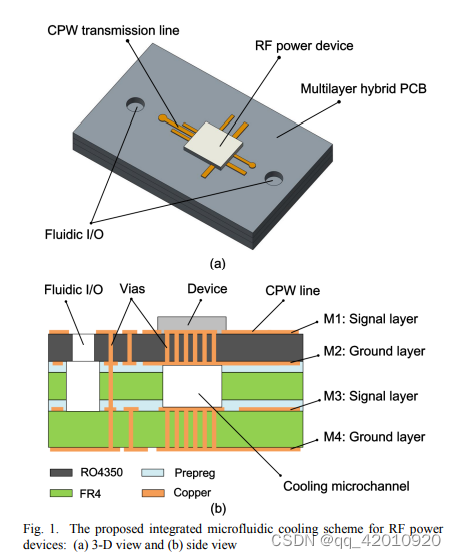
Fig. 1b shows the stack-up of the four-layer Rogers and FR4 hybrid PCB, which is a basic example of the scheme. In order to balance the cost and the RF performance, the top dielectric layer is made of a relatively low-cost high-frequency dielectric material (Rogers RO4350B) with a relative permittivity of 3.48 and a loss tangent of 0.0037 at 10 GHz, on which the RF transmission lines such as coplanar waveguide (CPW) lines and the corresponding RF components are realized, while the dielectric material of other layers is chosen as FR4 epoxy. The FR4 substrates, which are probably the most widely used and much cheaper than the RO4350B ones, are used to route the low frequency signals (e.g. power and control signals) and to fabricate the trench structure, as shown in Fig. 2c. The top dielectric layer (Rogers RO4350B), whose thickness is chosen as 508μm, is rigid enough so that the micochannel structure will not sag or collapse during the lamination process. Another concern is that the copper vias under the RF power devices must be solid, which is important for sealing the coolant fluid and enhancing both the thermal conductivity and the grounding performance.
fabrication
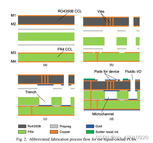
具有冷却微通道的四层混合PCB的制造过程完全基于标准的多层PCB技术,如图2所示。首先,厚度为0.508 mm的Rogers RO4350B覆铜板(CCL),两个FR4制备了 CCL 和一些预浸板。一个FR4 CCL,厚度为300 μm,用于形成冷却微通道的图案,其两侧的铜层被蚀刻掉,另一个厚度为1 mm,作为机械支撑和电互连,如图 2a 所示。随后,在顶部和底部层压板上钻出电气和流体通孔,然后在通孔侧壁上沉积几微米厚的铜层。接下来,RF 器件下方的接地通孔用铜膏填充并固化。同时,在中间FR4层压板和预浸片上加工微通道图案。
为了避免预浸料在层压过程中溢出到微通道中,预浸料上的微通道图案比FR4层压板上的微通道图案稍宽,如图2b所示。在底部 FR4 基板上的金属图案和通孔制作完成后,通过层压这两个 FR4 层压板来创建沟槽结构。为了防止在最外层铜层(即 M1 和 M4)的蚀刻过程中腐蚀内层铜层(即 M2 和 M3),然后在这些暴露区域的内层铜上电镀 500 nm 厚的金层,如图 2c 所示。接下来,通过沟槽结构和顶部RO4350B层压板的层压形成PCB微通道结构。在制作最外层铜层和铜通孔的图案后,分别沉积阻焊层和金层。洗涤后,最终得到混合 PCB,如图 2d 所示。图 3 显示了制造的四层 RO4350B 和 FR4 混合 PCB,包括流体 I/O、50 Ω CPW 线、阻抗匹配图案以及射频和功率信号的焊盘。 PCB 的重量为 25 g,尺寸为 73×68×2 mm3。流体 I/O 的直径为 2 mm。由 X 射线相机拍摄的插图显示了冷却微通道和铜通孔阵列。可以看出,微通道边缘到预浸料层边缘大约有1mm的距离,这在上面提到的图2b中,并且器件下方的过孔是实心的,而其他接地过孔与直径为 550 μm 的中空。图 4 显示了微通道、铜通孔阵列和流体 I/O 的细节。在这种情况下,微通道的横截面宽度为 2.17 mm,高度为 450 μm,而通孔直径和间距分别为 400 μm 和 560 μm。图 4b 显示嵌入式微通道的形状几乎是矩形。同时,微通道上的铜通孔填充质量好,未观察到空洞。值得一提的是,冷却液直接接触FR4基板的沟槽壁会吸收水分,因此在长期使用过程中可能存在可靠性问题。未来的工作可以集中在引入聚合物涂层工艺以提高与 PCB 基板吸水性相关的长期可靠性。
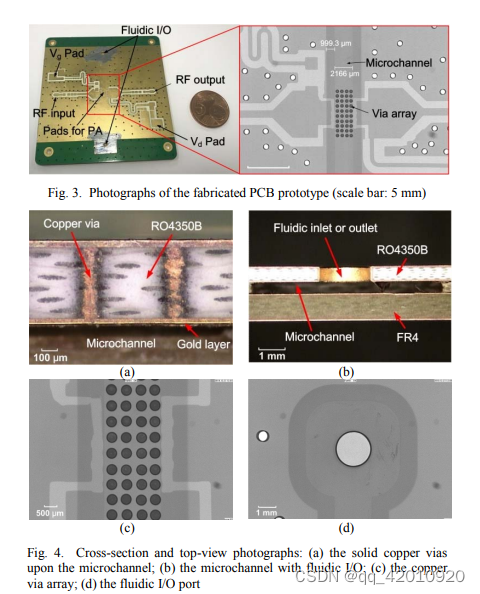
The fabrication process of the four-layer hybrid PCB with cooling microchannels is completely based on the standard multilayer PCB technology, as shown in Fig. 2. First, a Rogers RO4350B copper clad laminate (CCL) with a thickness of 0.508 mm, two FR4 CCLs and some prepreg sheets were prepared. One FR4 CCL, having a thickness of 300 μm, was used to form the pattern of the cooling microchannels, whose copper layers from both sides are etched out, and the other one having a thickness of 1 mm serves as mechanical support and electrical interconnection, as shown in Fig. 2a. Subsequently, the electrical and fluidic vias were drilled on top and bottom laminates and then a severalmicron-thick copper layer was deposited on the via sidewall. Next, the ground vias under the RF device were filled with copper paste and cured. Meanwhile, the microchannel pattern was machined on the middle FR4 laminate and the prepreg sheets. In order to avoid the prepreg material overflowing into the microchannel during lamination, the microchannel pattern on the prepregs was a little wider than that on the FR4 laminate, as shown in Fig. 2b. After the metal pattern and vias on the bottom FR4 substrate were fabricated, the trench structure was created by lamination of these two FR4 laminates. To prevent the corrosion of the inner copper layers (i.e., M2 and M3) during the etching of the outermost copper layers (i.e., M1 and M4), the inner copper at these exposed areas was then electroplated with a 500-nm-thick gold layer, as shown in Fig. 2c. Next, the PCB microchannel structure was formed by lamination of the trench structure and the top RO4350B laminate. After the patterns of the outermost copper layers and the copper vias were fabricated, a solder resist layer and a gold layer were deposited, respectively. After washing, the hybrid PCBs were finally obtained, as shown in Fig. 2d. Fig. 3 shows the fabricated four-layer RO4350B and FR4 hybrid PCB, including the fluidic I/O, the 50 Ω CPW lines, the patterns for impedance matching and the pads for the RF and power signals. The PCB has a weight of 25 g and a size of 73×68×2 mm3 . The diameter of the fluidic I/O is 2 mm. The inset picture, taken by an X-Ray camera, shows the cooling microchannel and the copper via array. It can been seen that there is a distance of about 1 mm from the edge of the microchannel to that of the prepreg layer, which is mentioned above as in Fig. 2b, and the vias under the device are solid, while other ground vias with a diameter of 550 μm are hollow. Fig. 4 shows the details of the microchannel, the copper via array and the fluidic I/O. In this case, the cross section of microchannel has a width of 2.17 mm and a height of 450 μm, while the via diameter and pitch are 400 μm and 560 μm, respectively. Fig. 4b shows that the embedded microchannel is almost rectangular in shape. Meanwhile, the copper vias upon the microchannel have good filling quality and no voids are observed. It is worth to mention that the coolant directly touches the trench walls of FR4 substrates that will absorb the water, so there may be problems with reliability during longterm use. Future work could focus on introducing polymer coating process to improve the long-term reliability related to the water absorption of PCB substrates.
measurment
NXP Semiconductors 的塑料 10 W 横向扩散金属氧化物半导体 (LDMOS) 功率晶体管器件 (BLP7G22-10) 用于执行热和射频测试,工作频率范围为 700 MHz 至 2700 MHz。射频功率放大器、电阻器和电容器使用回流工艺安装在制造的 PCB 原型上,然后将电镀有镍层的流体连接器手动焊接在流体 I/O 端口处。图 5 显示了组装后的 PCB 原型。实验装置如图 6 所示。对于 RF 部分,Agilent E8267D 信号发生器用于生成 2.1 GHz 的单音 CW 信号。 Qorvo 的 2 W 驱动放大器 (TQP9221) 在 2.1 GHz 时具有 31.2 dB 的增益,用于提高功率放大器的输入功率水平。功率放大器的输出信号衰减 30 dB,然后馈入 Agilent E4447A 频谱分析仪。两条带有 SMA 连接器的 50 Ω 同轴电缆手动焊接在 PCB 上的 RF 焊盘上,用于功率放大器的输入和输出。对于液体冷却系统,去离子(DI)水用作冷却剂,由齿轮泵(GA-V21-DEMSE micropump inc. USA)循环,而100目过滤器用于过滤杂质。两个K型热电偶分别安装在功放器件表面和PCB地平面上,用数字温度计(RS 55II温度计)测量温度。实验在 290 K 的室温下进行。
A plastic 10 W lateral diffused metal-oxide semiconductor (LDMOS) power transistor device (BLP7G22-10) from NXP Semiconductors, having a working frequency ranging from 700 MHz to 2700 MHz, was used to perform the thermal and RF tests. The RF power amplifier, resistors and capacitors were mounted on the fabricated PCB prototype using the reflow process, and then the fluidic connectors electroplated with a nickel layer were manually soldered at the fluidic I/O ports. Fig. 5 shows the PCB prototype after the assembly. The experimental setup is shown in Fig. 6. For the RF part, the Agilent E8267D signal generator was used to generate a single-tone CW signal at 2.1 GHz. A 2 W drive amplifier (TQP9221) from Qorvo, having a gain of 31.2 dB at 2.1 GHz, was used to improve the input power level of the power amplifier. The output signal of the power amplifier was attenuated by 30 dB and then fed into the Agilent E4447A spectrum analyzer. Two 50 Ω coaxial cables with SMA connectors were manually soldered at the RF pads on the PCB for the input and output of the power amplifier. For the liquid cooling system, deionized (DI) water was used as coolant, which was circulated by a gear pump (GA-V21-DEMSE micropump inc. USA), while a 100-mesh strainer was used to filter impurities. Two K-type thermocouples were mounted on the surface of the power amplifier device and the PCB ground plane, respectively, and the temperature was measured by a digital thermometer (RS 55II thermometer). The experiments were performed at room temperature of 290 K.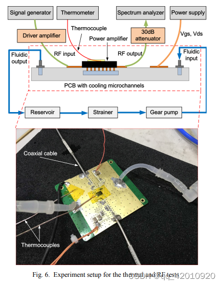
In this case, the total power consumption of the power amplifier is 26.32 W, while the RF output power is 41.2 dBm (13.2 W). Therefore, it can be calculated that the thermal power of the power amplifier is 13.12 W and the equivalent heat flux for the plastic package is 54.7 W/cm
Fig. 7 presents transient response of the case temperature of the power amplifier for different coolant flow rate. It can be observed that the case temperature rises rapidly within about 10 seconds and gradually becomes stable. As the coolant flow rate increases, the steady-state case temperature decreases. For example, the steady-state case temperature is 77.3 °C at the flow rate of 7.3 mL/min, and it is 55.7 °C at the flow rate of 84 mL/min. However, when the flow rate increases beyond 220 mL/min, the improvement of heat transfer performance is limited. For example, when the flow rate is set at 325 mL/min and 280 mL/min, respectively, the difference of their steadystate case temperatures is only 0.8 °C. According to the product data sheet of the power amplifier, the plastic package has a thermal resistance from junction to case of 3.2 K/W. It can be calculated that the junction temperature is 119.3 °C even with a relatively low flow rate of 7.3 mL/min, which is far below the limiting value of 150 °C. For comparison, the same assembled PCB was installed on a metal heat sink and also air-cooled by a fan. After power on, the case temperature of the power amplifier that output the same output power soared above 120 °C in about 10 seconds with a static fluid, and then the power amplifier failed soon
图 7 给出了功率放大器外壳温度对不同冷却液流量的瞬态响应。可以观察到外壳温度在大约10秒内迅速上升并逐渐趋于稳定。随着冷却剂流速的增加,稳态外壳温度降低。例如,流速为 7.3 mL/min 时的稳态壳体温度为 77.3 °C,流速为 84 mL/min 时为 55.7 °C。然而,当流速增加超过 220 mL/min 时,传热性能的提高是有限的。例如,当流速分别设置为 325 mL/min 和 280 mL/min 时,它们的稳态外壳温度差异仅为 0.8 °C。根据功率放大器的产品数据表,塑料封装从结到外壳的热阻为 3.2 K/W。可以计算得出,即使在 7.3 mL/min 的相对较低流速下,结温仍为 119.3 °C,远低于 150 °C 的极限值。作为比较,相同的组装 PCB 安装在金属散热器上,并通过风扇进行风冷。通电后,输出相同输出功率的功放机壳温度在静电液中10秒左右飙升至120℃以上,然后功放很快出现故障
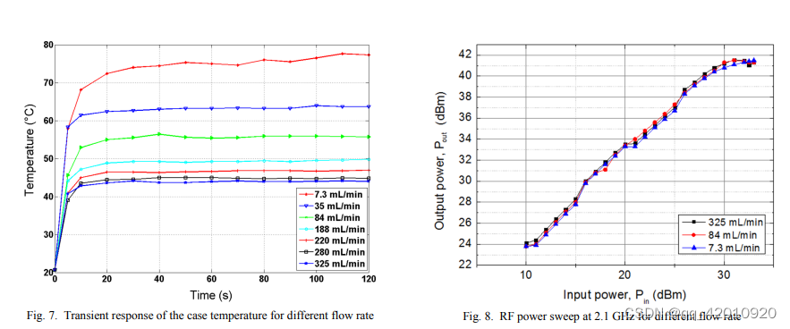
The power amplifier was matched to be operated at the frequency of 2.1 GHz. The CW output power of 41.2 dBm and the power-added efficiency (PAE) of 42.6% were obtained at Vgs=2.2V and Vds=28V. Fig. 8 shows the RF power sweep that was performed at 2.1 GHz. It can be observed that there is not much difference in the output power at the different water flow rate. During the whole experiment, no leakage of water has been observed.
RF模块输出功率没多大变化
This paper presents an integrated microfluidic channel on a hybrid PCB to cool an S-band 10 W CW power amplifier in a surface mount package. The four-layer Rogers RO4350B and FR4 hybrid PCB has been fabricated and tested. The thermal and RF experimental results shows that the integrated microfluidic cooling scheme on the multilayer hybrid PCB is effective. The CW output power of 41.2 dBm is obtained at 2.1 GHz, while the case temperature is 44 °C. The proposed liquid-cooled PCBs offer the advantages of low cost, low profile and high cooling capacity, which can be used for high power RF applications.
这篇关于Integrated Microfluidic Cooling for S-Band 10-Watt CW Power Amplifiers on Hybrid PCBs的文章就介绍到这儿,希望我们推荐的文章对编程师们有所帮助!


