本文主要是介绍STM32存储左右互搏 SPI总线读写FLASH W25QXX,希望对大家解决编程问题提供一定的参考价值,需要的开发者们随着小编来一起学习吧!
STM32存储左右互搏 SPI总线读写FLASH W25QXX
FLASH是常用的一种非易失存储单元,W25QXX系列Flash有不同容量的型号,如W25Q64的容量为64Mbit,也就是8MByte。这里介绍STM32CUBEIDE开发平台HAL库操作W25Q各型号FLASH的例程。
W25QXX介绍
W25QXX的SOIC封装如下所示,在采用SPI而不是QUAL SPI时,管脚定义为:

即由片选(/CS), 时钟(CLK), 数据输出(DO)和数据输入(DI)的组成4线SPI信号接口。VCC和GND提供电源和接地连接。
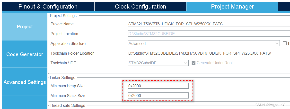
例程采用STM32H750VBT6芯片, FLASH可以选择为8/16/32/64/128/256/512/1024 Mbit的W25Q型号。
STM32工程配置
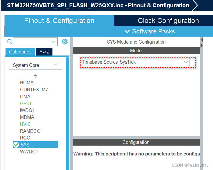
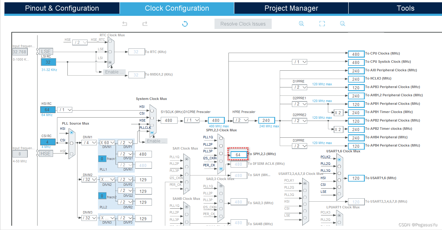
首先建立基本工程并设置时钟:
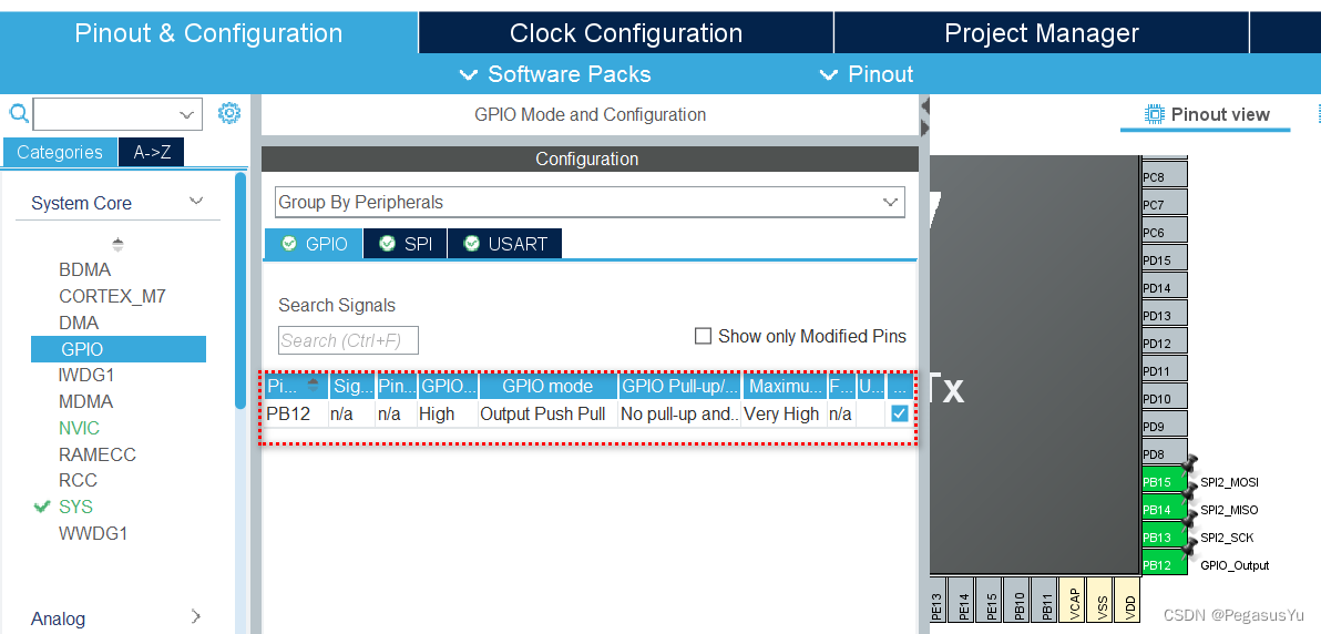
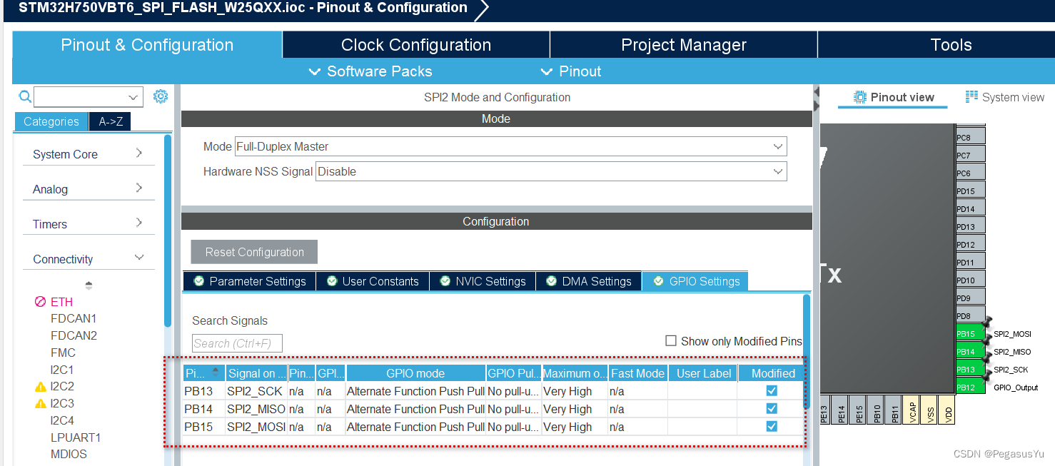
选择硬件接口SPI2为FLASH连接接口,片选采用软件代码控制方式,单独设置为输出GPIO:
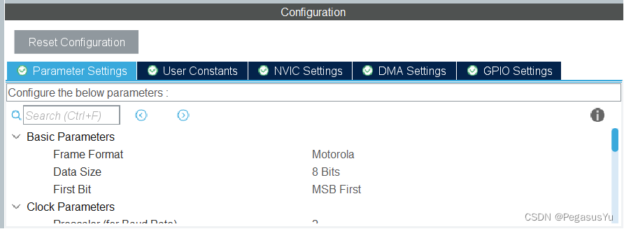
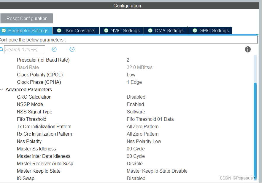
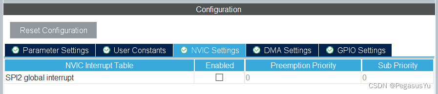
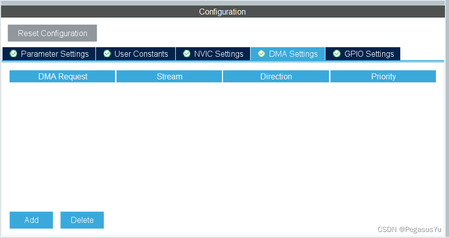
不采用中断和DMA方式,需要时可以再添加,调用相对应的操作库函数及补充中断处理函数即可。
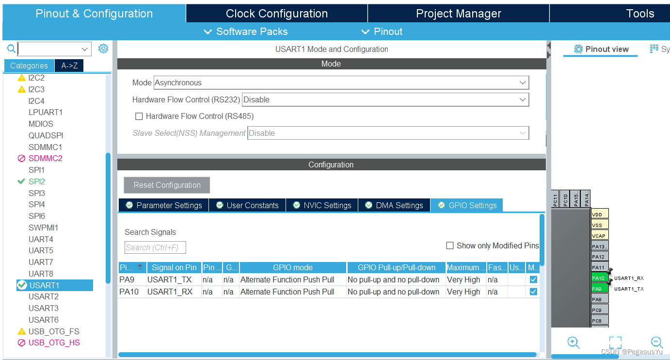
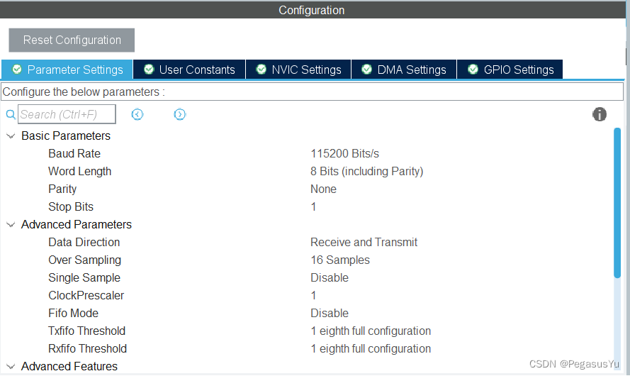
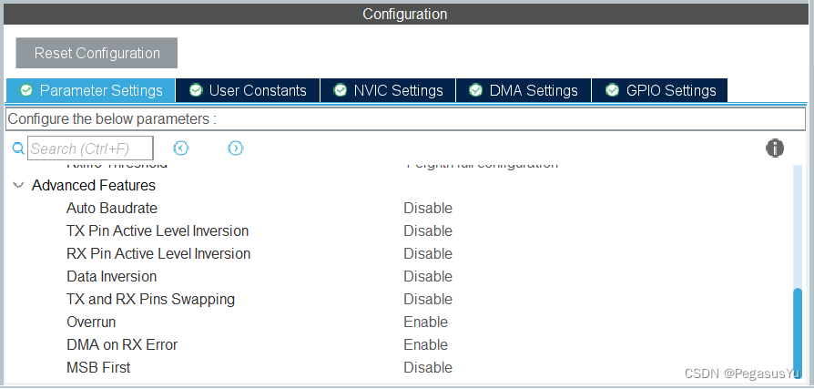
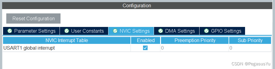
配置UART1用于控制打印:
STM32H7资源较多,可以将堆栈开大:
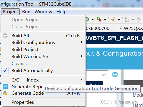
保存并生成初始工程代码:
STM32工程代码
UART串口printf打印输出实现参考:STM32 UART串口printf函数应用及浮点打印代码空间节省 (HAL)
建立W25Q访问的库头文件W25QXX.h:
#ifndef INC_W25QXX_H_
#define INC_W25QXX_H_#include "main.h"uint8_t SPI2_ReadWriteByte(uint8_t TxData);//W25QXX serial chip list:
#define W25Q20_ID 	0XEF11
#define W25Q40_ID 	0XEF12
#define W25Q80_ID 	0XEF13
#define W25Q16_ID 	0XEF14
#define W25Q32_ID 	0XEF15
#define W25Q64_ID 	0XEF16
#define W25Q128_ID	0XEF17
#define W25Q256_ID	0XEF18
#define W25Q512_ID  0XEF19
#define W25Q1024_ID 0XEF20extern uint16_t W25QXX_TYPE; //To indicate W25QXX type used in this procedure//W25QXX chip select control function
#define W25QXX_CS(n)  ( n ? HAL_GPIO_WritePin(GPIOB, GPIO_PIN_12, GPIO_PIN_SET) : HAL_GPIO_WritePin(GPIOB, GPIO_PIN_12, GPIO_PIN_RESET) )//command table for W25QXX access
#define W25X_WriteEnable		0x06
#define W25X_WriteDisable		0x04
#define W25X_ReadStatusReg1		0x05
#define W25X_ReadStatusReg2		0x35
#define W25X_ReadStatusReg3		0x15
#define W25X_WriteStatusReg1    0x01
#define W25X_WriteStatusReg2    0x31
#define W25X_WriteStatusReg3    0x11
#define W25X_ReadData			0x03
#define W25X_FastReadData		0x0B
#define W25X_FastReadDual		0x3B
#define W25X_PageProgram		0x02
#define W25X_BlockErase			0xD8
#define W25X_SectorErase		0x20
#define W25X_ChipErase			0xC7
#define W25X_PowerDown			0xB9
#define W25X_ReleasePowerDown	0xAB
#define W25X_DeviceID			0xAB
#define W25X_ManufactDeviceID	0x90
#define W25X_JedecDeviceID		0x9F
#define W25X_Enable4ByteAddr    0xB7
#define W25X_Exit4ByteAddr      0xE9uint8_t W25QXX_Init(void);
uint16_t  W25QXX_ReadID(void);  	    		  //Read W25QXX ID
uint8_t W25QXX_ReadSR(uint8_t reg_num);           //Read from status register
void W25QXX_4ByteAddr_Enable(void);               //Enable 4-byte address mode
void W25QXX_Write_SR(uint8_t reg_num,uint8_t d);  //Write to status register
void W25QXX_Write_Enable(void);  		          //Write enable
void W25QXX_Write_Disable(void);		          //Write disable
void W25QXX_Write_NoCheck(uint8_t* pBuffer,uint32_t WriteAddr,uint16_t NumByteToWrite); //Write operation w/o check
void W25QXX_Read(uint8_t* pBuffer,uint32_t ReadAddr,uint16_t NumByteToRead);            //Read operation
void W25QXX_Write(uint8_t* pBuffer,uint32_t WriteAddr,uint16_t NumByteToWrite);         //Write operation
void W25QXX_Erase_Chip(void);    	  	                                                //Erase whole chip
void W25QXX_Erase_Sector(uint32_t Sector_Num);	                                        //Erase sector in specific sector number
void W25QXX_Wait_Busy(void);           	       //Wait idle status before next operation
void W25QXX_PowerDown(void);        	       //Enter power-down mode
void W25QXX_WAKEUP(void);				       //Wake-up#endif /* INC_W25QXX_H_ */
建立W25Q访问的库源文件W25QXX.c:
#include "W25QXX.h"extern SPI_HandleTypeDef hspi2;
extern void PY_Delay_us_t(uint32_t Delay);
//Write and read one byte in SPI2
uint8_t SPI2_ReadWriteByte(uint8_t TxData)
{uint8_t Rxdata;HAL_SPI_TransmitReceive(&hspi2,&TxData,&Rxdata,1, 1000);return Rxdata;
}uint16_t W25QXX_TYPE=W25Q64_ID;//W25QXX initialization
uint8_t W25QXX_Init(void)
{uint8_t temp;W25QXX_CS(1);W25QXX_TYPE=W25QXX_ReadID();if((W25QXX_TYPE==W25Q256_ID)||(W25QXX_TYPE==W25Q512_ID)||(W25QXX_TYPE==W25Q1024_ID)){temp=W25QXX_ReadSR(3);              //read status register 3if((temp&0X01)==0)			        //judge address mode and configure to 4-byte address mode{W25QXX_CS(0);SPI2_ReadWriteByte(W25X_Enable4ByteAddr);W25QXX_CS(1);}}if((W25QXX_TYPE==0x0000)||(W25QXX_TYPE==0xFFFF)) return 0;else return 1;
}//Read status registers of W25QXX
//reg_num: register number from 1 to 3
//return: value of selected register//SR1 (default 0x00):
//BIT7  6   5   4   3   2   1   0
//SPR   RV  TB BP2 BP1 BP0 WEL BUSY
//SPR: default 0, status register protection bit used with WP
//TB,BP2,BP1,BP0: FLASH region write protection configuration
//WEL: write enable lock
//BUSY: busy flag (1: busy; 0: idle)//SR2:
//BIT7  6   5   4   3   2   1   0
//SUS   CMP LB3 LB2 LB1 (R) QE  SRP1//SR3:
//BIT7      6    5    4   3   2   1   0
//HOLD/RST  DRV1 DRV0 (R) (R) WPS ADP ADS
uint8_t W25QXX_ReadSR(uint8_t reg_num)
{uint8_t byte=0,command=0;switch(reg_num){case 1:command=W25X_ReadStatusReg1;    //To read status register 1break;case 2:command=W25X_ReadStatusReg2;    //To read status register 2break;case 3:command=W25X_ReadStatusReg3;    //To read status register 3break;default:command=W25X_ReadStatusReg1;break;}W25QXX_CS(0);SPI2_ReadWriteByte(command);    //send commandbyte=SPI2_ReadWriteByte(0Xff);  //read dataW25QXX_CS(1);return byte;
}//Write status registers of W25QXX
//reg_num: register number from 1 to 3
//d: data for updating status register
void W25QXX_Write_SR(uint8_t reg_num,uint8_t d)
{uint8_t command=0;switch(reg_num){case 1:command=W25X_WriteStatusReg1;    //To write status register 1break;case 2:command=W25X_WriteStatusReg2;    //To write status register 2break;case 3:command=W25X_WriteStatusReg3;    //To write status register 3break;default:command=W25X_WriteStatusReg1;break;}W25QXX_CS(0);SPI2_ReadWriteByte(command);            //send commandSPI2_ReadWriteByte(d);                  //write dataW25QXX_CS(1);
}
//W25QXX write enable
void W25QXX_Write_Enable(void)
{W25QXX_CS(0);SPI2_ReadWriteByte(W25X_WriteEnable);W25QXX_CS(1);
}
//W25QXX write disable
void W25QXX_Write_Disable(void)
{W25QXX_CS(0);SPI2_ReadWriteByte(W25X_WriteDisable);W25QXX_CS(1);
}//Read chip ID
//return:
//0XEF11 for W25Q20
//0XEF12 for W25Q40
//0XEF13 for W25Q80
//0XEF14 for W25Q16
//0XEF15 for W25Q32
//0XEF16 for W25Q64
//0XEF17 for W25Q128
//0XEF18 for W25Q256
uint16_t W25QXX_ReadID(void)
{uint16_t Temp = 0;W25QXX_CS(0);SPI2_ReadWriteByte(0x90);          //send commandSPI2_ReadWriteByte(0x00);SPI2_ReadWriteByte(0x00);SPI2_ReadWriteByte(0x00);Temp|=SPI2_ReadWriteByte(0xFF)<<8; //read high byte dataTemp|=SPI2_ReadWriteByte(0xFF);    //read low byte dataW25QXX_CS(1);return Temp;
}
//Read W25QXX from specific address for specific byte length
//pBuffer: data buffer
//ReadAddr: specific address
//NumByteToRead: specific byte length (max 65535)
void W25QXX_Read(uint8_t* pBuffer,uint32_t ReadAddr,uint16_t NumByteToRead)
{uint16_t i;W25QXX_CS(0);SPI2_ReadWriteByte(W25X_ReadData);                   //send read commandif((W25QXX_TYPE==W25Q256_ID)||(W25QXX_TYPE==W25Q512_ID)||(W25QXX_TYPE==W25Q1024_ID))   //send highest 8-bit address{SPI2_ReadWriteByte((uint8_t)((ReadAddr)>>24));}SPI2_ReadWriteByte((uint8_t)((ReadAddr)>>16));       //send 24-bit addressSPI2_ReadWriteByte((uint8_t)((ReadAddr)>>8));SPI2_ReadWriteByte((uint8_t)ReadAddr);for(i=0;i<NumByteToRead;i++){pBuffer[i]=SPI2_ReadWriteByte(0XFF);             //read data}W25QXX_CS(1);
}//Write W25QXX not more than 1 page (256 bytes)
//pBuffer: data buffer
//WriteAddr: specific address
//NumByteToWrite: specific byte length (max 256)
void W25QXX_Write_Page(uint8_t* pBuffer,uint32_t WriteAddr,uint16_t NumByteToWrite)
{uint16_t i;W25QXX_Write_Enable();                                       //write enableW25QXX_CS(0);SPI2_ReadWriteByte(W25X_PageProgram);                        //send write commandif((W25QXX_TYPE==W25Q256_ID)||(W25QXX_TYPE==W25Q512_ID)||(W25QXX_TYPE==W25Q1024_ID))  //send highest 8-bit address{SPI2_ReadWriteByte((uint8_t)((WriteAddr)>>24));}SPI2_ReadWriteByte((uint8_t)((WriteAddr)>>16));               //send 24-bit addressSPI2_ReadWriteByte((uint8_t)((WriteAddr)>>8));SPI2_ReadWriteByte((uint8_t)WriteAddr);for(i=0;i<NumByteToWrite;i++)SPI2_ReadWriteByte(pBuffer[i]);  //write dataW25QXX_CS(1);W25QXX_Wait_Busy();
}//Write W25QXX w/o erase check and w/o byte number restriction
//pBuffer: data buffer
//WriteAddr: specific address
//NumByteToWrite: specific byte length (max 65535)
void W25QXX_Write_NoCheck(uint8_t* pBuffer,uint32_t WriteAddr,uint16_t NumByteToWrite)
{uint16_t remained_byte_num_in_page;remained_byte_num_in_page=256-WriteAddr%256;                                                       //remained byte number in pageif( NumByteToWrite <= remained_byte_num_in_page ) remained_byte_num_in_page = NumByteToWrite;      //data can be written in single pagewhile(1){W25QXX_Write_Page(pBuffer,WriteAddr,remained_byte_num_in_page);if(NumByteToWrite==remained_byte_num_in_page)break;                                            //end write operationelse                                                                                           //NumByteToWrite>remained_byte_num_in_page{pBuffer+=remained_byte_num_in_page;WriteAddr+=remained_byte_num_in_page;NumByteToWrite-=remained_byte_num_in_page;if(NumByteToWrite>256)remained_byte_num_in_page=256;                                       //for whole page writeelse remained_byte_num_in_page=NumByteToWrite; 	                                           //for non-whole page write}};
}//Write W25QXX w/ erase after check and w/o byte number restriction
//pBuffer: data buffer
//WriteAddr: specific address
//NumByteToWrite: specific byte length (max 65535)
uint8_t W25QXX_BUFFER[4096];
void W25QXX_Write(uint8_t* pBuffer,uint32_t WriteAddr,uint16_t NumByteToWrite)
{uint32_t secpos;uint16_t secoff;uint16_t secremain;uint16_t i;uint8_t * W25QXX_BUF;W25QXX_BUF=W25QXX_BUFFER;secpos=WriteAddr/4096;                                        //sector number (16 pages for 1 sector) for destination addresssecoff=WriteAddr%4096;                                        //offset address in sector for destination addresssecremain=4096-secoff;                                        //remained space for sectorif(NumByteToWrite<=secremain)secremain=NumByteToWrite;        //data can be written in single sectorwhile(1){W25QXX_Read(W25QXX_BUF,secpos*4096,4096);                 //read sector data for ease necessity judgmentfor(i=0;i<secremain;i++)                                  //check sector data status{if(W25QXX_BUF[secoff+i]!=0XFF) break;                 //ease necessary}if(i<secremain)                                           //for ease{W25QXX_Erase_Sector(secpos);                          //ease sectorfor(i=0;i<secremain;i++)	                          //data copy{W25QXX_BUF[i+secoff]=pBuffer[i];}W25QXX_Write_NoCheck(W25QXX_BUF,secpos*4096,4096);     //write sector}else W25QXX_Write_NoCheck(pBuffer,WriteAddr,secremain);   //write data for sector unnecessary to eraseif(NumByteToWrite==secremain)break;                        //for operation endelse                                                       //for operation continuing{secpos++;                                              //sector number + 1secoff=0;                                              //offset address from 0pBuffer+=secremain;                                    //pointer adjustmentWriteAddr+=secremain;                                  //write address adjustmentNumByteToWrite-=secremain;				               //write number adjustmentif(NumByteToWrite>4096) secremain=4096;	               //not last sectorelse secremain=NumByteToWrite;			               //last sector}};
}//Erase whole chip, long waiting...
void W25QXX_Erase_Chip(void)
{W25QXX_Write_Enable();                  //write enableW25QXX_Wait_Busy();W25QXX_CS(0);SPI2_ReadWriteByte(W25X_ChipErase);     //send erase commandW25QXX_CS(1);W25QXX_Wait_Busy();   				    //wait for erase complete
}//Erase one sector
//Sector_Num: sector number
void W25QXX_Erase_Sector(uint32_t Sector_Num)
{Sector_Num*=4096;W25QXX_Write_Enable();                                     //write enableW25QXX_Wait_Busy();W25QXX_CS(0);SPI2_ReadWriteByte(W25X_SectorErase);                      //send erase commandif((W25QXX_TYPE==W25Q256_ID)||(W25QXX_TYPE==W25Q512_ID)||(W25QXX_TYPE==W25Q1024_ID))  //send highest 8-bit address{SPI2_ReadWriteByte((uint8_t)((Sector_Num)>>24));}SPI2_ReadWriteByte((uint8_t)((Sector_Num)>>16));           //send 24-bit addressSPI2_ReadWriteByte((uint8_t)((Sector_Num)>>8));SPI2_ReadWriteByte((uint8_t)Sector_Num);W25QXX_CS(1);W25QXX_Wait_Busy();   				                       //wait for erase complete
}//Wait idle status before next operation
void W25QXX_Wait_Busy(void)
{while((W25QXX_ReadSR(1)&0x01)==0x01);    //wait for busy flag cleared
}//Enter power-down mode
#define tDP_us 3
void W25QXX_PowerDown(void)
{W25QXX_CS(0);SPI2_ReadWriteByte(W25X_PowerDown);      //send power-down commandW25QXX_CS(1);PY_Delay_us_t(tDP_us);                   //tDP
}
//Wake-up
#define tRES1_us 3
void W25QXX_WAKEUP(void)
{W25QXX_CS(0);SPI2_ReadWriteByte(W25X_ReleasePowerDown);//send release power-down commandW25QXX_CS(1);PY_Delay_us_t(tRES1_us);                  //tRES1
}main.c文件操作代码里实现串口接收1个字节的指令,实现FLASH的ID读取,一页的写入,一页的读出三个功能。其它功能可以根据需要自行增加。
/* USER CODE BEGIN Header */
/********************************************************************************* @file           : main.c* @brief          : Main program body******************************************************************************* @attention** Copyright (c) 2023 STMicroelectronics.* All rights reserved.** This software is licensed under terms that can be found in the LICENSE file* in the root directory of this software component.* If no LICENSE file comes with this software, it is provided AS-IS.********************************************************************************/
//Written by Pegasus Yu in 2023
/* USER CODE END Header */
/* Includes ------------------------------------------------------------------*/
#include "main.h"/* Private includes ----------------------------------------------------------*/
/* USER CODE BEGIN Includes */
#include "usart.h"
#include "W25QXX.h"
#include <string.h>
/* USER CODE END Includes *//* Private typedef -----------------------------------------------------------*/
/* USER CODE BEGIN PTD */
__IO float usDelayBase;
void PY_usDelayTest(void)
{__IO uint32_t firstms, secondms;__IO uint32_t counter = 0;firstms = HAL_GetTick()+1;secondms = firstms+1;while(uwTick!=firstms) ;while(uwTick!=secondms) counter++;usDelayBase = ((float)counter)/1000;
}void PY_Delay_us_t(uint32_t Delay)
{__IO uint32_t delayReg;__IO uint32_t usNum = (uint32_t)(Delay*usDelayBase);delayReg = 0;while(delayReg!=usNum) delayReg++;
}void PY_usDelayOptimize(void)
{__IO uint32_t firstms, secondms;__IO float coe = 1.0;firstms = HAL_GetTick();PY_Delay_us_t(1000000) ;secondms = HAL_GetTick();coe = ((float)1000)/(secondms-firstms);usDelayBase = coe*usDelayBase;
}void PY_Delay_us(uint32_t Delay)
{__IO uint32_t delayReg;__IO uint32_t msNum = Delay/1000;__IO uint32_t usNum = (uint32_t)((Delay%1000)*usDelayBase);if(msNum>0) HAL_Delay(msNum);delayReg = 0;while(delayReg!=usNum) delayReg++;
}
/* USER CODE END PTD *//* Private define ------------------------------------------------------------*/
/* USER CODE BEGIN PD */
/* USER CODE END PD *//* Private macro -------------------------------------------------------------*/
/* USER CODE BEGIN PM *//* USER CODE END PM *//* Private variables ---------------------------------------------------------*/SPI_HandleTypeDef hspi2;UART_HandleTypeDef huart1;/* USER CODE BEGIN PV */
uint8_t uart1_rx[16];
uint8_t cmd;
uint32_t Flash_Access_Addr = 0;
/* USER CODE END PV *//* Private function prototypes -----------------------------------------------*/
void SystemClock_Config(void);
void PeriphCommonClock_Config(void);
static void MX_GPIO_Init(void);
static void MX_USART1_UART_Init(void);
static void MX_SPI2_Init(void);
/* USER CODE BEGIN PFP *//* USER CODE END PFP *//* Private user code ---------------------------------------------------------*/
/* USER CODE BEGIN 0 */
#define page_byte_size 256
uint8_t sdbuffer[page_byte_size];
/* USER CODE END 0 *//*** @brief  The application entry point.* @retval int*/
int main(void)
{/* USER CODE BEGIN 1 *//* USER CODE END 1 *//* MCU Configuration--------------------------------------------------------*//* Reset of all peripherals, Initializes the Flash interface and the Systick. */HAL_Init();/* USER CODE BEGIN Init *//* USER CODE END Init *//* Configure the system clock */SystemClock_Config();/* Configure the peripherals common clocks */PeriphCommonClock_Config();/* USER CODE BEGIN SysInit *//* USER CODE END SysInit *//* Initialize all configured peripherals */MX_GPIO_Init();MX_USART1_UART_Init();MX_SPI2_Init();/* USER CODE BEGIN 2 */PY_usDelayTest();PY_usDelayOptimize();HAL_UART_Receive_IT(&huart1, uart1_rx, 1);W25QXX_Init();/* USER CODE END 2 *//* Infinite loop *//* USER CODE BEGIN WHILE */while (1){if(cmd==1) //Read ID{cmd = 0;printf("FLASH ID=0x%x\r\n\r\n", W25QXX_ReadID());printf("W25Q80_ID: 0XEF13\r\n");printf("W25Q16_ID: 0XEF14\r\n");printf("W25Q32_ID: 0XEF15\r\n");printf("W25Q64_ID: 0XEF16\r\n");printf("W25Q128_ID: 0XEF17\r\n");printf("W25Q256_ID: 0XEF18\r\n");printf("W25Q512_ID: 0XEF18\r\n");printf("W25Q1024_ID: 0XEF20\r\n");}if(cmd==2) //Write one page{cmd = 0;for(uint32_t i=0;i<page_byte_size;i++){sdbuffer[i]=i;}Flash_Access_Addr = 0;W25QXX_Write(sdbuffer, Flash_Access_Addr, page_byte_size);printf("Write to W25Q6XX done!\r\n");}if(cmd==3)//Read one page{cmd = 0;memset(sdbuffer, 0, page_byte_size);printf("Start to read W25QXX......\r\n");Flash_Access_Addr = 0;W25QXX_Read(sdbuffer, Flash_Access_Addr, page_byte_size);for(uint32_t i=0; i<page_byte_size; i++){printf("%d ", sdbuffer[i]);}printf("\r\n");}/* USER CODE END WHILE *//* USER CODE BEGIN 3 */}/* USER CODE END 3 */
}/*** @brief System Clock Configuration* @retval None*/
void SystemClock_Config(void)
{RCC_OscInitTypeDef RCC_OscInitStruct = {0};RCC_ClkInitTypeDef RCC_ClkInitStruct = {0};/** Supply configuration update enable*/HAL_PWREx_ConfigSupply(PWR_LDO_SUPPLY);/** Configure the main internal regulator output voltage*/__HAL_PWR_VOLTAGESCALING_CONFIG(PWR_REGULATOR_VOLTAGE_SCALE1);while(!__HAL_PWR_GET_FLAG(PWR_FLAG_VOSRDY)) {}__HAL_RCC_SYSCFG_CLK_ENABLE();__HAL_PWR_VOLTAGESCALING_CONFIG(PWR_REGULATOR_VOLTAGE_SCALE0);while(!__HAL_PWR_GET_FLAG(PWR_FLAG_VOSRDY)) {}/** Initializes the RCC Oscillators according to the specified parameters* in the RCC_OscInitTypeDef structure.*/RCC_OscInitStruct.OscillatorType = RCC_OSCILLATORTYPE_HSI;RCC_OscInitStruct.HSIState = RCC_HSI_DIV1;RCC_OscInitStruct.HSICalibrationValue = RCC_HSICALIBRATION_DEFAULT;RCC_OscInitStruct.PLL.PLLState = RCC_PLL_ON;RCC_OscInitStruct.PLL.PLLSource = RCC_PLLSOURCE_HSI;RCC_OscInitStruct.PLL.PLLM = 4;RCC_OscInitStruct.PLL.PLLN = 60;RCC_OscInitStruct.PLL.PLLP = 2;RCC_OscInitStruct.PLL.PLLQ = 2;RCC_OscInitStruct.PLL.PLLR = 2;RCC_OscInitStruct.PLL.PLLRGE = RCC_PLL1VCIRANGE_3;RCC_OscInitStruct.PLL.PLLVCOSEL = RCC_PLL1VCOWIDE;RCC_OscInitStruct.PLL.PLLFRACN = 0;if (HAL_RCC_OscConfig(&RCC_OscInitStruct) != HAL_OK){Error_Handler();}/** Initializes the CPU, AHB and APB buses clocks*/RCC_ClkInitStruct.ClockType = RCC_CLOCKTYPE_HCLK|RCC_CLOCKTYPE_SYSCLK|RCC_CLOCKTYPE_PCLK1|RCC_CLOCKTYPE_PCLK2|RCC_CLOCKTYPE_D3PCLK1|RCC_CLOCKTYPE_D1PCLK1;RCC_ClkInitStruct.SYSCLKSource = RCC_SYSCLKSOURCE_PLLCLK;RCC_ClkInitStruct.SYSCLKDivider = RCC_SYSCLK_DIV1;RCC_ClkInitStruct.AHBCLKDivider = RCC_HCLK_DIV2;RCC_ClkInitStruct.APB3CLKDivider = RCC_APB3_DIV2;RCC_ClkInitStruct.APB1CLKDivider = RCC_APB1_DIV2;RCC_ClkInitStruct.APB2CLKDivider = RCC_APB2_DIV2;RCC_ClkInitStruct.APB4CLKDivider = RCC_APB4_DIV2;if (HAL_RCC_ClockConfig(&RCC_ClkInitStruct, FLASH_LATENCY_4) != HAL_OK){Error_Handler();}
}/*** @brief Peripherals Common Clock Configuration* @retval None*/
void PeriphCommonClock_Config(void)
{RCC_PeriphCLKInitTypeDef PeriphClkInitStruct = {0};/** Initializes the peripherals clock*/PeriphClkInitStruct.PeriphClockSelection = RCC_PERIPHCLK_CKPER;PeriphClkInitStruct.CkperClockSelection = RCC_CLKPSOURCE_HSI;if (HAL_RCCEx_PeriphCLKConfig(&PeriphClkInitStruct) != HAL_OK){Error_Handler();}
}/*** @brief SPI2 Initialization Function* @param None* @retval None*/
static void MX_SPI2_Init(void)
{/* USER CODE BEGIN SPI2_Init 0 *//* USER CODE END SPI2_Init 0 *//* USER CODE BEGIN SPI2_Init 1 *//* USER CODE END SPI2_Init 1 *//* SPI2 parameter configuration*/hspi2.Instance = SPI2;hspi2.Init.Mode = SPI_MODE_MASTER;hspi2.Init.Direction = SPI_DIRECTION_2LINES;hspi2.Init.DataSize = SPI_DATASIZE_8BIT;hspi2.Init.CLKPolarity = SPI_POLARITY_LOW;hspi2.Init.CLKPhase = SPI_PHASE_1EDGE;hspi2.Init.NSS = SPI_NSS_SOFT;hspi2.Init.BaudRatePrescaler = SPI_BAUDRATEPRESCALER_2;hspi2.Init.FirstBit = SPI_FIRSTBIT_MSB;hspi2.Init.TIMode = SPI_TIMODE_DISABLE;hspi2.Init.CRCCalculation = SPI_CRCCALCULATION_DISABLE;hspi2.Init.CRCPolynomial = 0x0;hspi2.Init.NSSPMode = SPI_NSS_PULSE_ENABLE;hspi2.Init.NSSPolarity = SPI_NSS_POLARITY_LOW;hspi2.Init.FifoThreshold = SPI_FIFO_THRESHOLD_01DATA;hspi2.Init.TxCRCInitializationPattern = SPI_CRC_INITIALIZATION_ALL_ZERO_PATTERN;hspi2.Init.RxCRCInitializationPattern = SPI_CRC_INITIALIZATION_ALL_ZERO_PATTERN;hspi2.Init.MasterSSIdleness = SPI_MASTER_SS_IDLENESS_00CYCLE;hspi2.Init.MasterInterDataIdleness = SPI_MASTER_INTERDATA_IDLENESS_00CYCLE;hspi2.Init.MasterReceiverAutoSusp = SPI_MASTER_RX_AUTOSUSP_DISABLE;hspi2.Init.MasterKeepIOState = SPI_MASTER_KEEP_IO_STATE_DISABLE;hspi2.Init.IOSwap = SPI_IO_SWAP_DISABLE;if (HAL_SPI_Init(&hspi2) != HAL_OK){Error_Handler();}/* USER CODE BEGIN SPI2_Init 2 *//* USER CODE END SPI2_Init 2 */}/*** @brief USART1 Initialization Function* @param None* @retval None*/
static void MX_USART1_UART_Init(void)
{/* USER CODE BEGIN USART1_Init 0 *//* USER CODE END USART1_Init 0 *//* USER CODE BEGIN USART1_Init 1 *//* USER CODE END USART1_Init 1 */huart1.Instance = USART1;huart1.Init.BaudRate = 115200;huart1.Init.WordLength = UART_WORDLENGTH_8B;huart1.Init.StopBits = UART_STOPBITS_1;huart1.Init.Parity = UART_PARITY_NONE;huart1.Init.Mode = UART_MODE_TX_RX;huart1.Init.HwFlowCtl = UART_HWCONTROL_NONE;huart1.Init.OverSampling = UART_OVERSAMPLING_16;huart1.Init.OneBitSampling = UART_ONE_BIT_SAMPLE_DISABLE;huart1.Init.ClockPrescaler = UART_PRESCALER_DIV1;huart1.AdvancedInit.AdvFeatureInit = UART_ADVFEATURE_NO_INIT;if (HAL_UART_Init(&huart1) != HAL_OK){Error_Handler();}if (HAL_UARTEx_SetTxFifoThreshold(&huart1, UART_TXFIFO_THRESHOLD_1_8) != HAL_OK){Error_Handler();}if (HAL_UARTEx_SetRxFifoThreshold(&huart1, UART_RXFIFO_THRESHOLD_1_8) != HAL_OK){Error_Handler();}if (HAL_UARTEx_DisableFifoMode(&huart1) != HAL_OK){Error_Handler();}/* USER CODE BEGIN USART1_Init 2 *//* USER CODE END USART1_Init 2 */}/*** @brief GPIO Initialization Function* @param None* @retval None*/
static void MX_GPIO_Init(void)
{GPIO_InitTypeDef GPIO_InitStruct = {0};/* GPIO Ports Clock Enable */__HAL_RCC_GPIOB_CLK_ENABLE();__HAL_RCC_GPIOA_CLK_ENABLE();/*Configure GPIO pin Output Level */HAL_GPIO_WritePin(GPIOB, GPIO_PIN_12, GPIO_PIN_SET);/*Configure GPIO pin : PB12 */GPIO_InitStruct.Pin = GPIO_PIN_12;GPIO_InitStruct.Mode = GPIO_MODE_OUTPUT_PP;GPIO_InitStruct.Pull = GPIO_NOPULL;GPIO_InitStruct.Speed = GPIO_SPEED_FREQ_VERY_HIGH;HAL_GPIO_Init(GPIOB, &GPIO_InitStruct);}/* USER CODE BEGIN 4 */
void HAL_UART_RxCpltCallback(UART_HandleTypeDef *huart)
{if(huart==&huart1){cmd = uart1_rx[0];HAL_UART_Receive_IT(&huart1, uart1_rx, 1);}}
/* USER CODE END 4 *//*** @brief  This function is executed in case of error occurrence.* @retval None*/
void Error_Handler(void)
{/* USER CODE BEGIN Error_Handler_Debug *//* User can add his own implementation to report the HAL error return state */__disable_irq();while (1){}/* USER CODE END Error_Handler_Debug */
}#ifdef  USE_FULL_ASSERT
/*** @brief  Reports the name of the source file and the source line number*         where the assert_param error has occurred.* @param  file: pointer to the source file name* @param  line: assert_param error line source number* @retval None*/
void assert_failed(uint8_t *file, uint32_t line)
{/* USER CODE BEGIN 6 *//* User can add his own implementation to report the file name and line number,ex: printf("Wrong parameters value: file %s on line %d\r\n", file, line) *//* USER CODE END 6 */
}
#endif /* USE_FULL_ASSERT */
STM32例程测试
串口指令0x01测试效果如下:
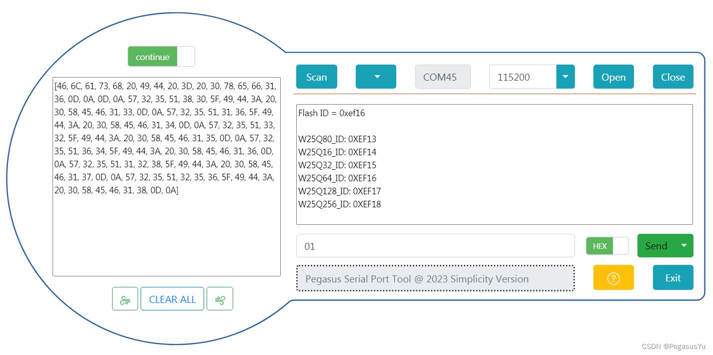
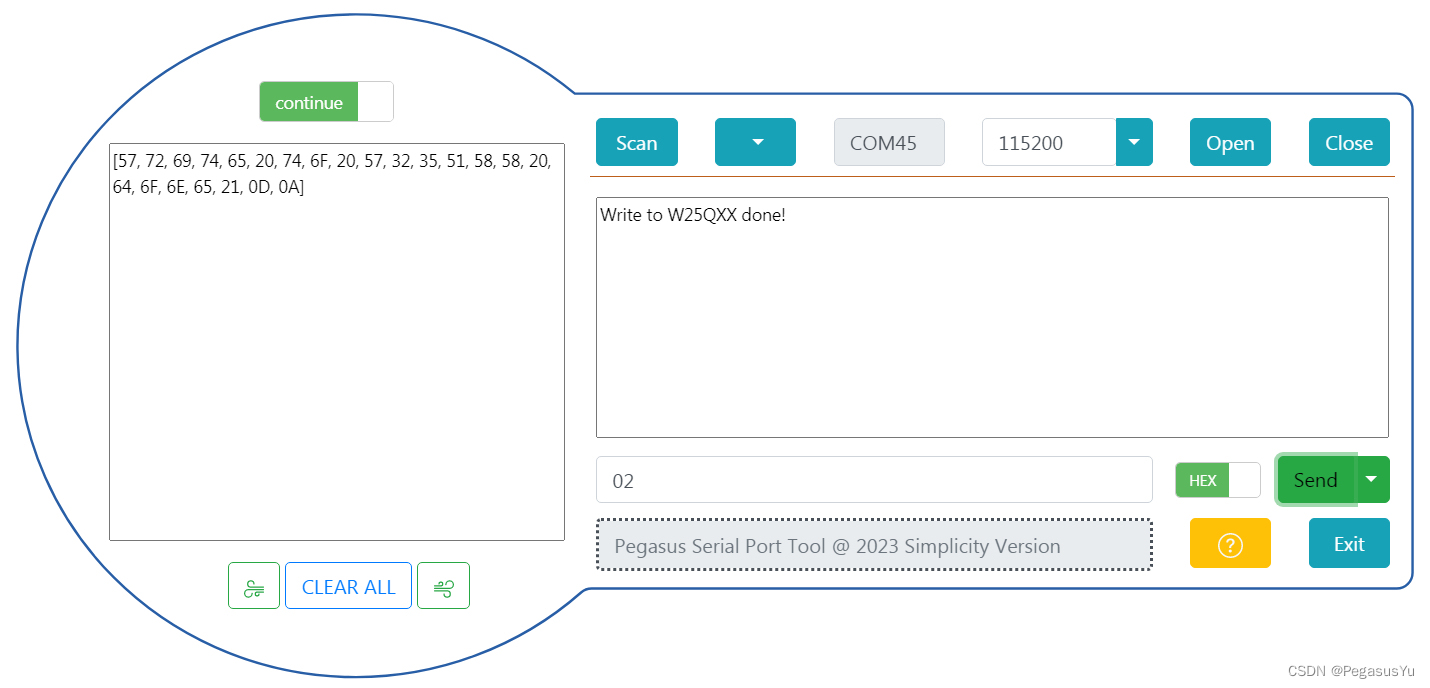
串口指令0x02测试效果如下:
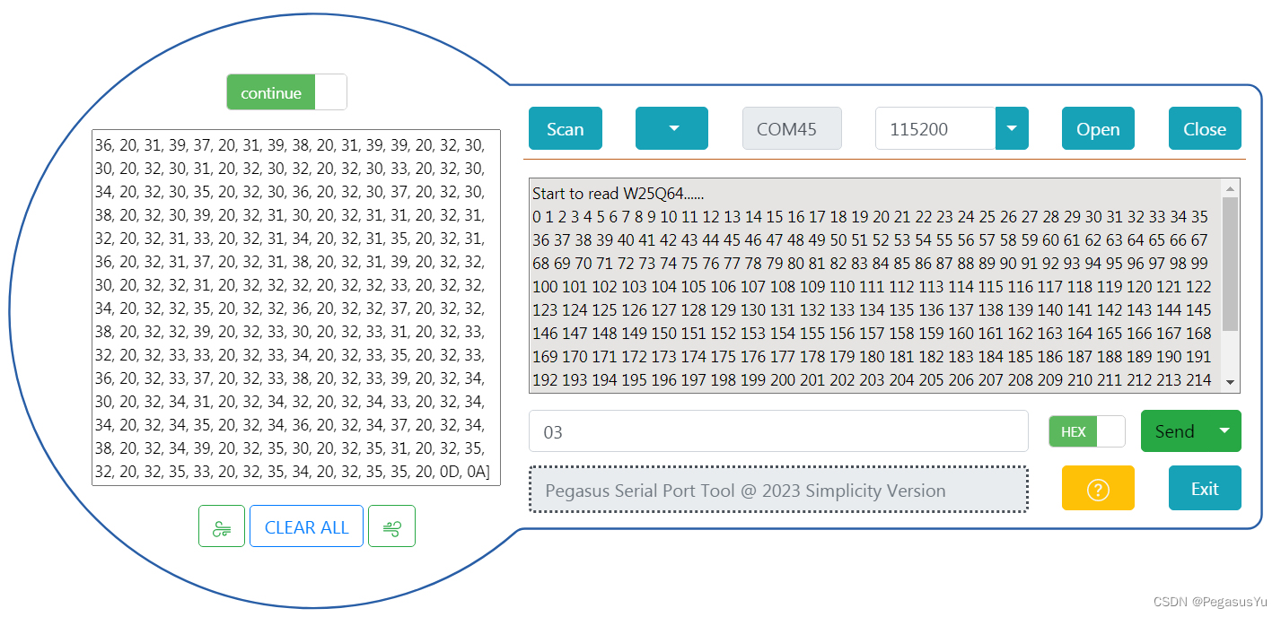
串口指令0x03测试效果如下:
STM32例程下载
STM32H750VBT6读写W25QXX例程下载
–End–
这篇关于STM32存储左右互搏 SPI总线读写FLASH W25QXX的文章就介绍到这儿,希望我们推荐的文章对编程师们有所帮助!