本文主要是介绍hcs12 microcontroller 笔记,希望对大家解决编程问题提供一定的参考价值,需要的开发者们随着小编来一起学习吧!
文章来由
来到美国后,选了微处理器课,有幸老教授是 MIT 贝尔实验室出来的,希望好好学习这门课。
零、Chapter 0 绪论
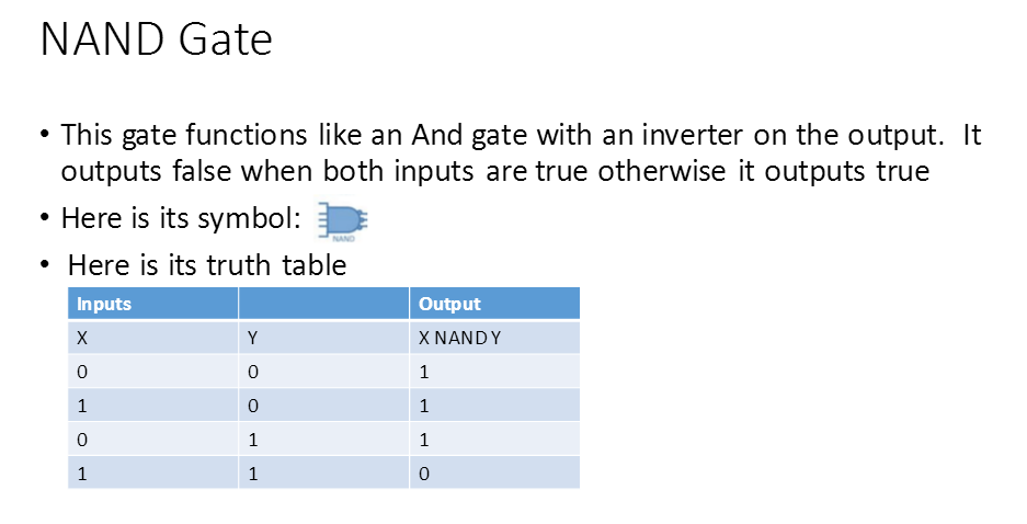
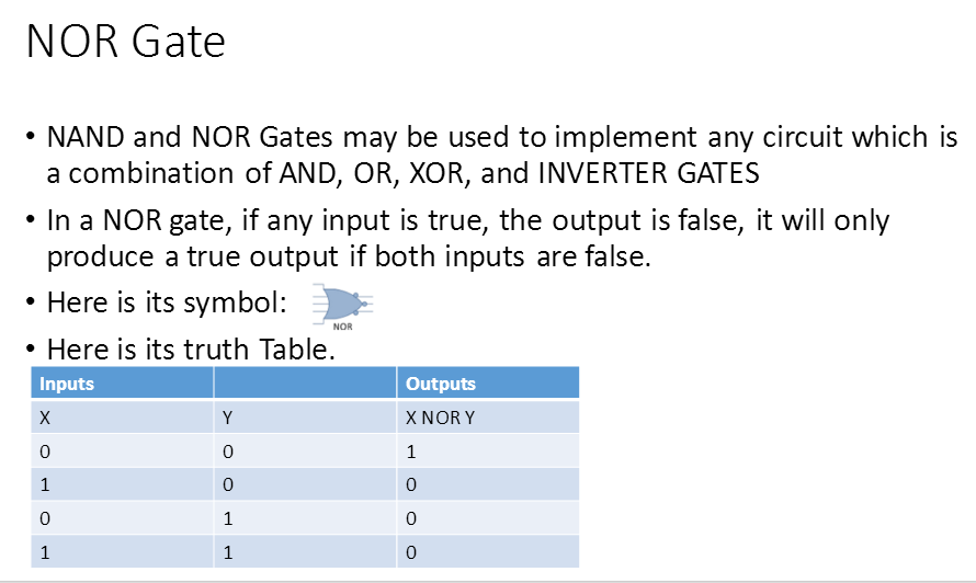
0-2 Logic Gates
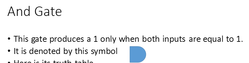
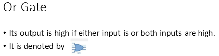
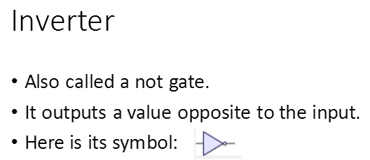
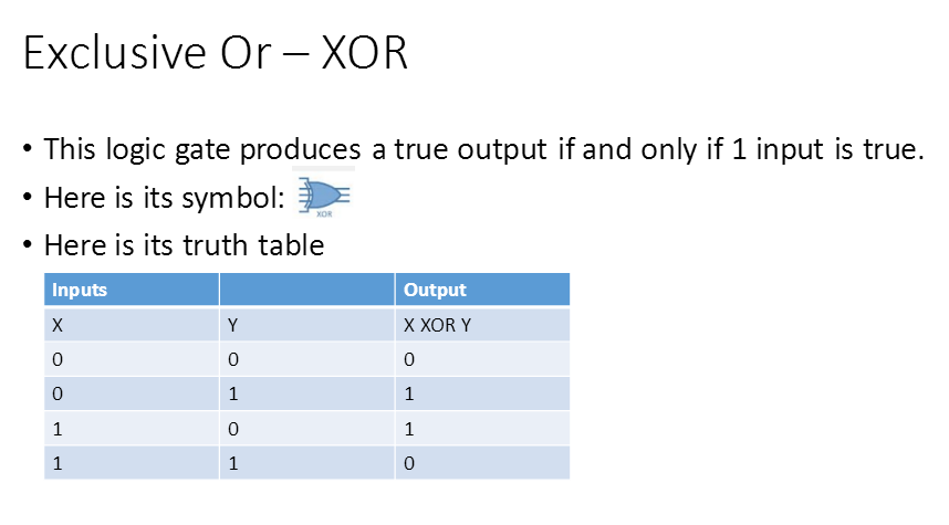
1、基础逻辑门(注意记住符号)
2、三态缓冲器
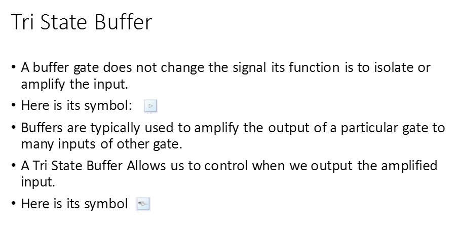
三态缓冲器(Three-state buffer),又称为三态门、三态驱动器,其三态输出受到使能输出端的控制,当使能输出有效时,器件实现正常逻辑状态输出(逻辑0、逻辑1),当使能输入无效时,输出处于高阻状态,即等效于与所连的电路断开。
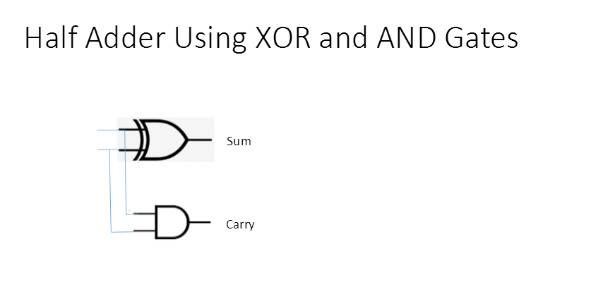
3、Logic Design using Gates 为什么可以用 and 做 carry
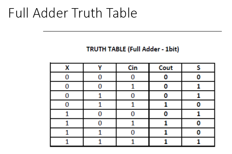
•Note that there are 4 possible outcomes when adding a pair of binary numbers
•0 + 0 = carry 0, sum 0
•0 + 1 = carry 0, sum 1
•1 + 0 = carry 0, sum 1
•1 + 1 = carry 1, sum 0
•Recall that the AND gate only outputs 1 if both inputs are true, thus it could be used to output the carry bit.
•Recall that the XOR gate only outputs 1 if and only if one of the inputs are true.
4、半加器
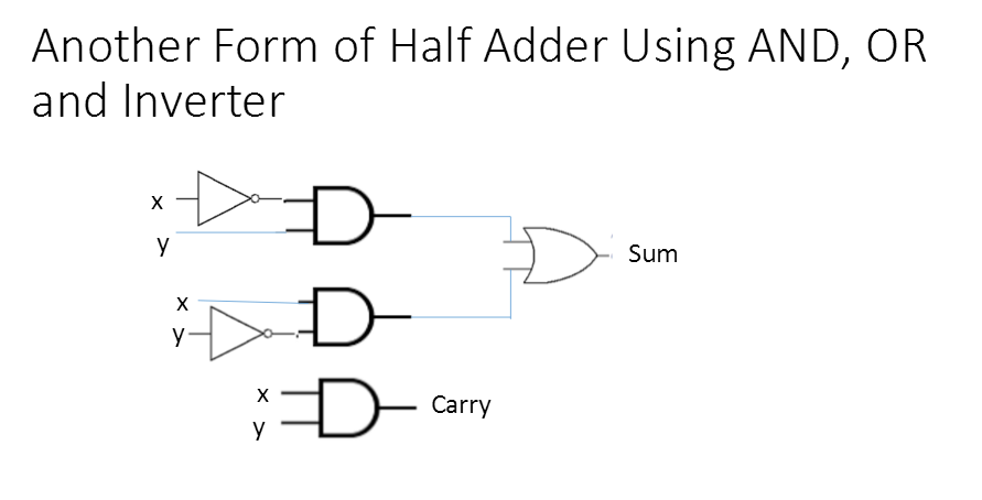
另一种形式

5、全加器
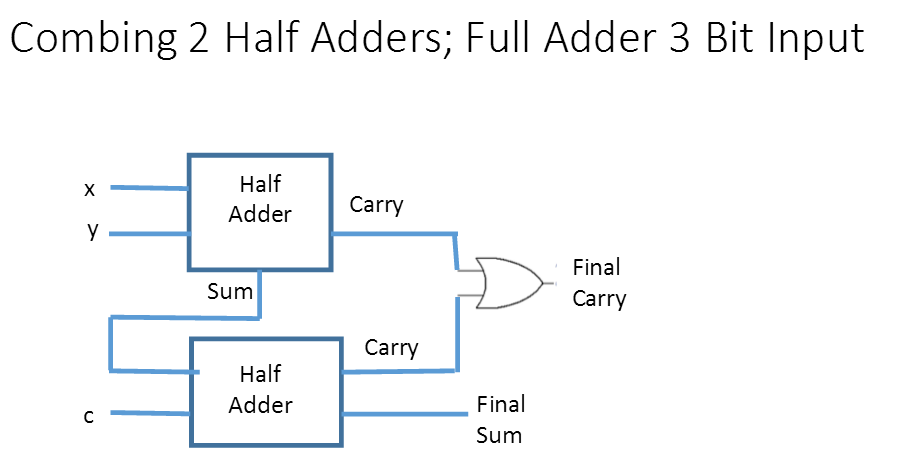
6、三位全加器
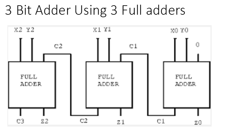
Application of the previous 3 Bit Adder
•Assume we want to add the binary numbers 010 and 011..
•Using the truth table shows before..
•We know that 0+1 with no carry in will result in Sum of 1 with no carry
•Also, 1+1 with no carry in will result in sum of 0 with carry out of 1 •Finally, 0+0 with carry in will result in sum of 1 with no carry
•Result is 0101
•The take away here is that we can cascade as many full adders as we want to add as large of a pair of binary numbers as we want.
•For example a 64 bit sum would require 64 cascaded adders
0-3 Semiconductor Memory(ROM、RAM类型)
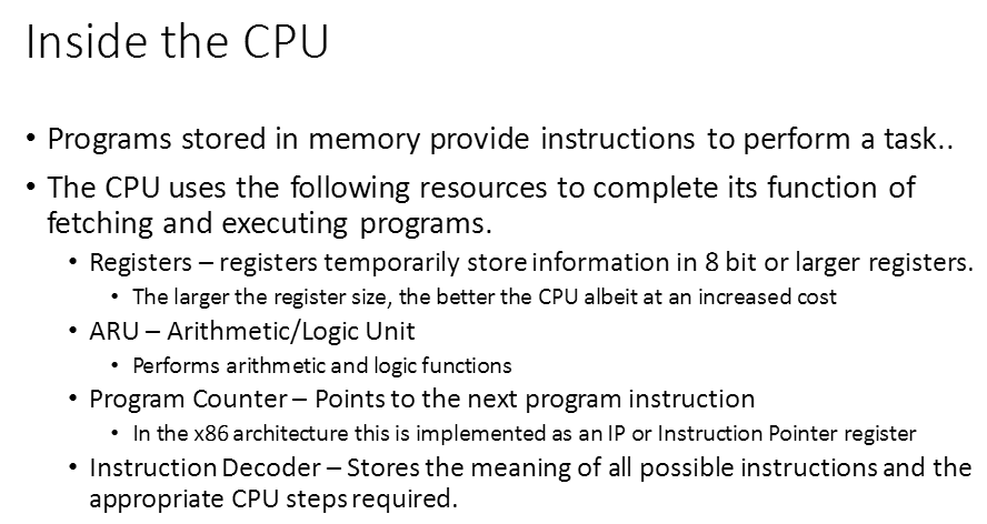
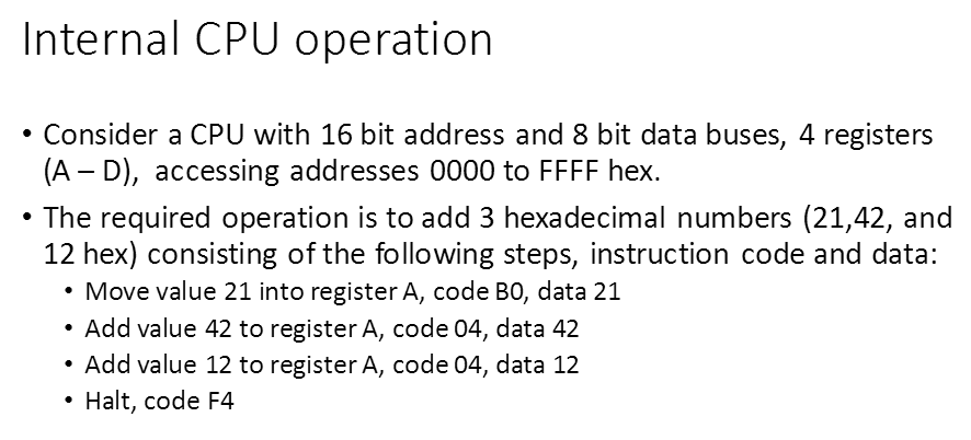
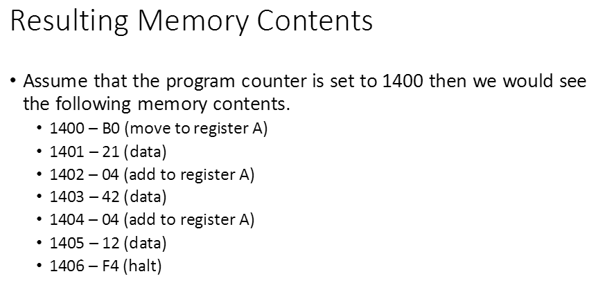
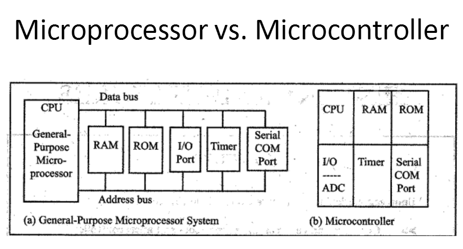
1、Internal Organization of computers
•3 major subsystems
•CPU – Central Processing Unit •Memory •I/O Input Output
•Connected by buses
•Data •Address •Control
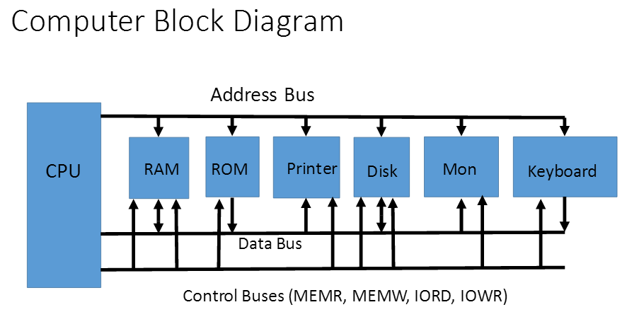
More About the Data Bus
•Analogous to Highway
•The more lanes, the more simultaneous traffic
•The more data buses the better
•This adds to expense
•Note that we currently have 64 bit CPUs and operating systems
•The size of the data bus is related to both size and precisions of arithmetic operations
More About the Address Bus
•Every addressable device must have a unique address
•The larger the address bus, the larger number of devices which may be addressed by the CPU
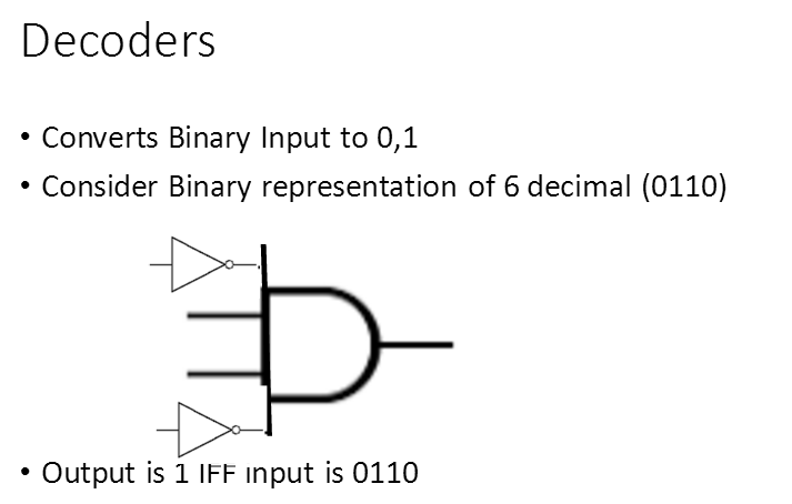
•Recall that decoders are used on addressable device to establish their address.
•The number of devices which may be addressed is always equal to 2^x where x is the number of address lines.
•For example, a 16 bit address bus can access 64k of addressable memory
•This is a unidirectional bus (send only from CPU)
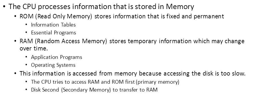
2、Relation of CPU to RAM and ROM
3、Memory Capacity
•This is the number of bits a memory chip can store
•Chip capacity has units of bits, Computer system capacity has units of bytes
4、Memory Organization
•Memory chips are organized into a number of locations within the IC
•Each location can hold 1, 4, 8, 16, or more bits
•The number of bits that each location will hold is equal to the number of data
pins on the chip.
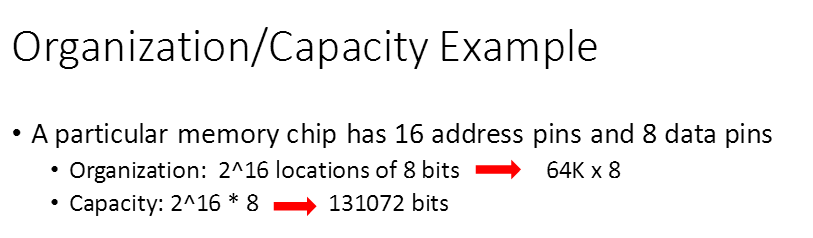
•The number of locations on the chip is determined by the number of address pins on the chip say x. 2^x is the number of locations (addresses) on the chip
•Total number of bits which may be stored on the entire chip is given by 2^(address pins) times the number of data pins
Another Organization/Capacity Example
•We have a chip with 256k capacity with 8 data pins.
•The organization is 256k/8 = 32K x 8 •The number of address lines is 15 since 2^15 = 32K
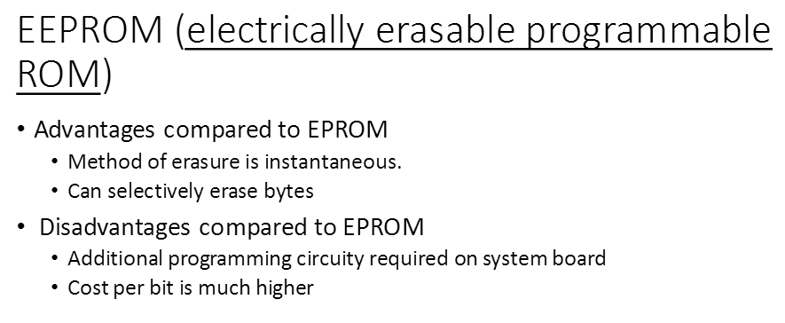
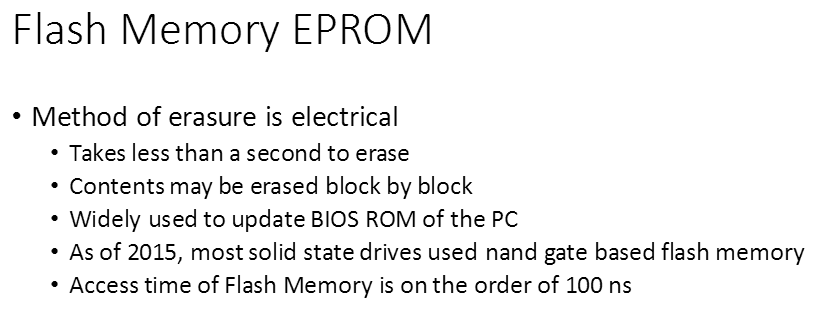
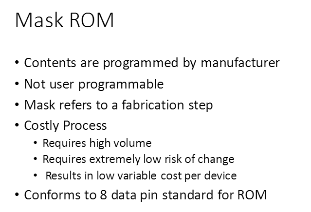
5、不同ROM类型
Different types such as:
•PROM
•EPROM
•EEPROM
•FLASH EPROM
•MASK PROM
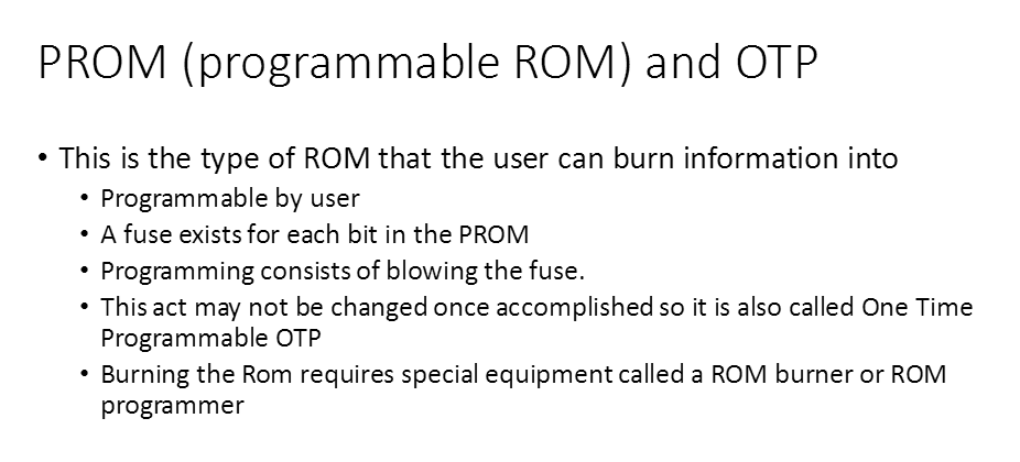
(1)PROM (programmable ROM) and OTP
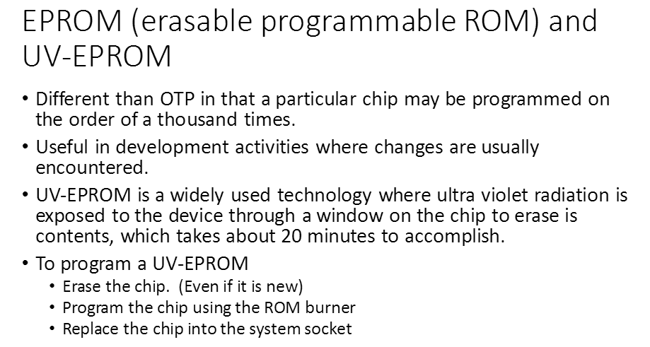
(2)EPROM (erasable programmable ROM) and UV-EPROM
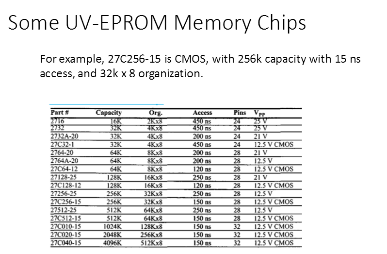
(3)Some UV-EPROM Memory Chips obsolete 已过时
(4)EEPROM (electrically erasable programmable ROM)
(5)Flash Memory EPROM
(6)Mask ROM
6、不同RAM类型
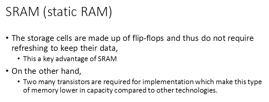
3 types
•Static RAM
•Nonvolatile RAM
•Dynamic Ram
(1)SRAM (static RAM)
(2)NV-RAM (nonvolatile RAM)

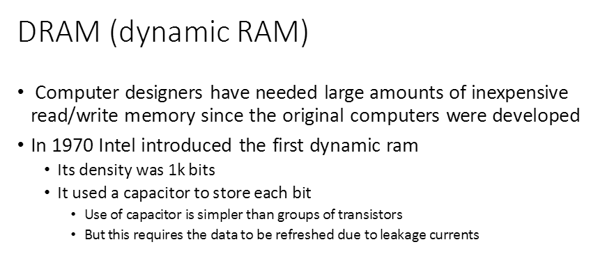
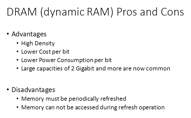
(3)DRAM (dynamic RAM)
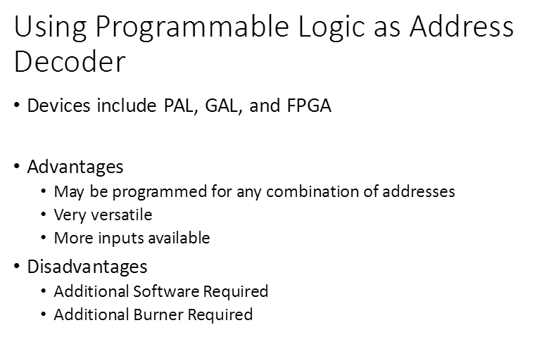
7、Memory Block Selection
•Simple Logic Gates
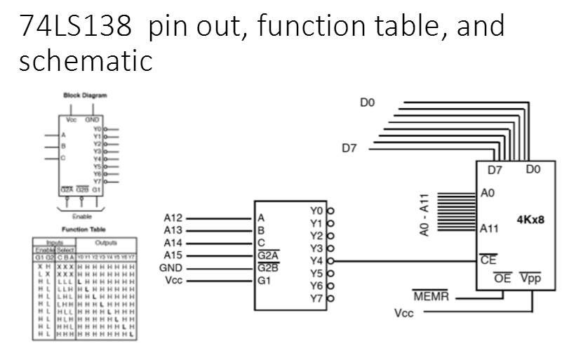
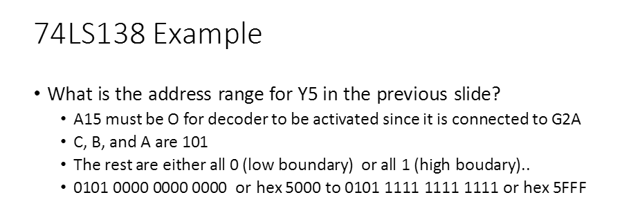
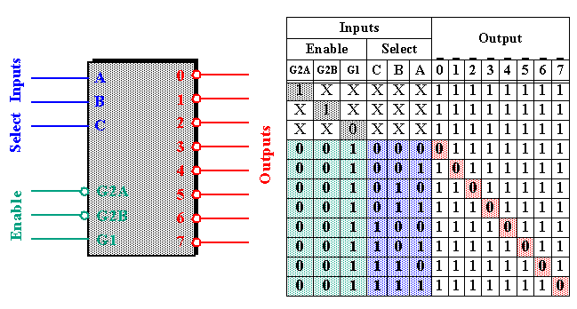
•Using 74LS138
•Programmable Logic such as CPLD or FPGA
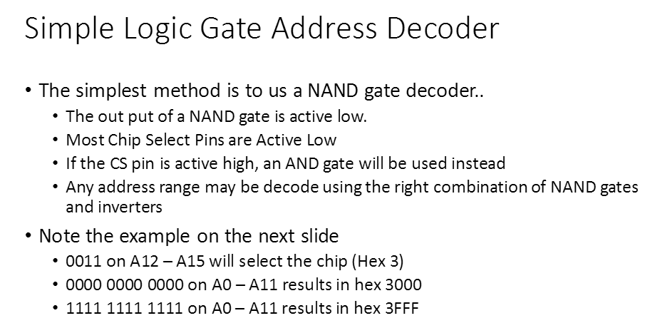
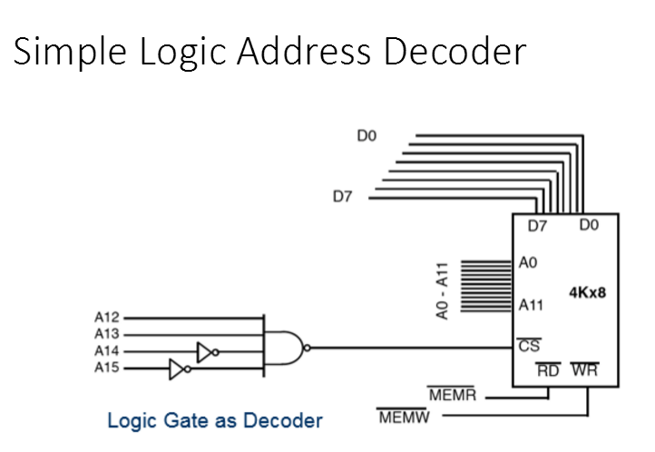
详见:http://blog.csdn.net/scythe666/article/details/52428243
Using the 74LS138 3 – 8 decoder
•One of the most widely used decoders •3 inputs A, B, and C generate 8 active low outputs Y0 to Y7, •Each output is connected to CS of a different memory device allowing
control of 8 memory blocks
•Three additional inputs G1, G2A, and G2B may connected to an Address or Control Signal
•G2A and G2B active low •G1 active high •These inputs must be terminated in way or another •These inputs enable the device
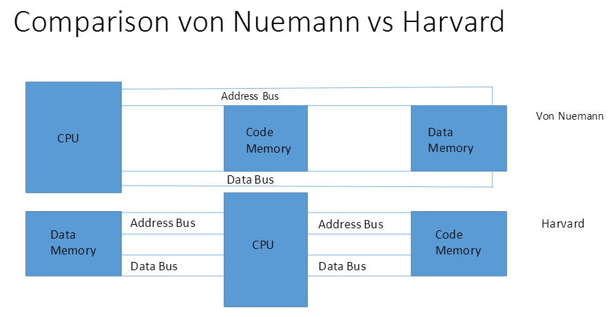
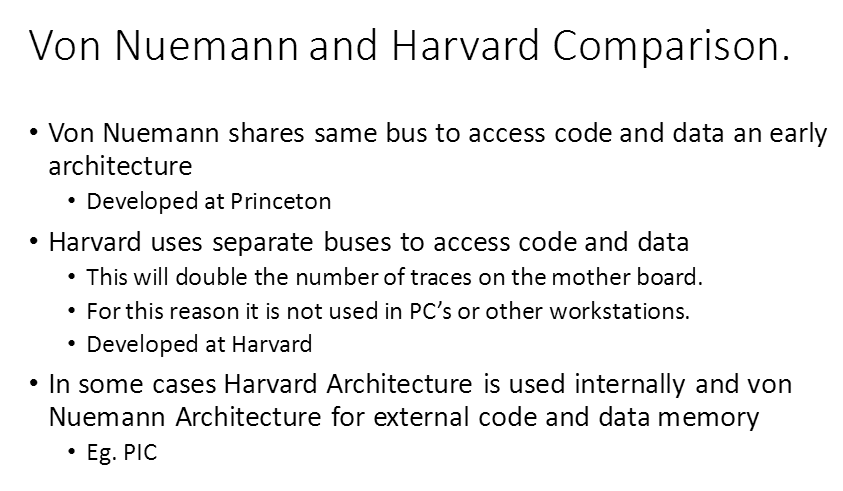
0-4 Harvard and von Neumann CPU Architectures
一、Chapter 1 微处理器简史
二、Chapter 2 内存 寄存器 简单指令
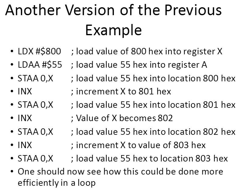
2-1 Registers of HCS12
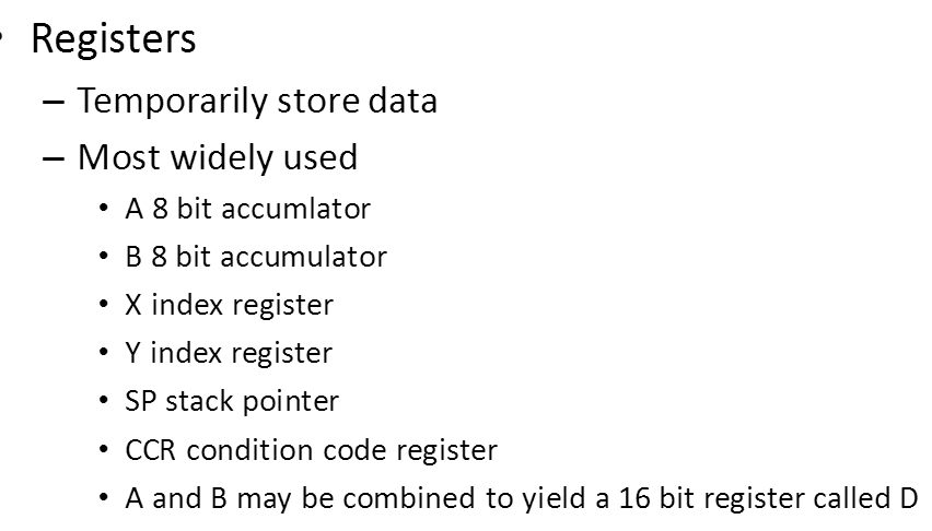
1、Registers overview
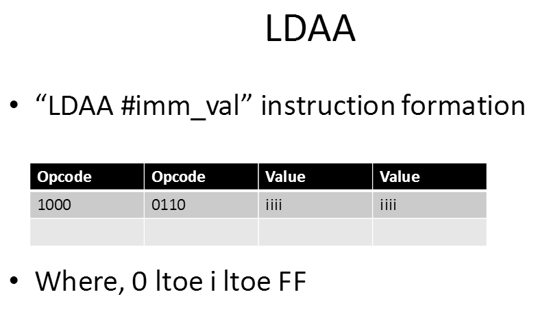
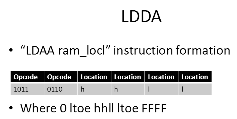
LDAA #$35 ; loads 55 hex into Accumulator A
•# signifies an immediate value
•$ signifies that the immediate value is base 16
Absence of the # sign indicates that the value should be loaded from a memory location
•Eg LDAA $17 will load the contents of memory location 17 hex
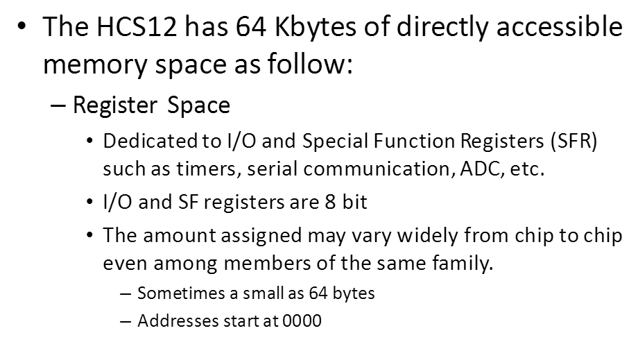
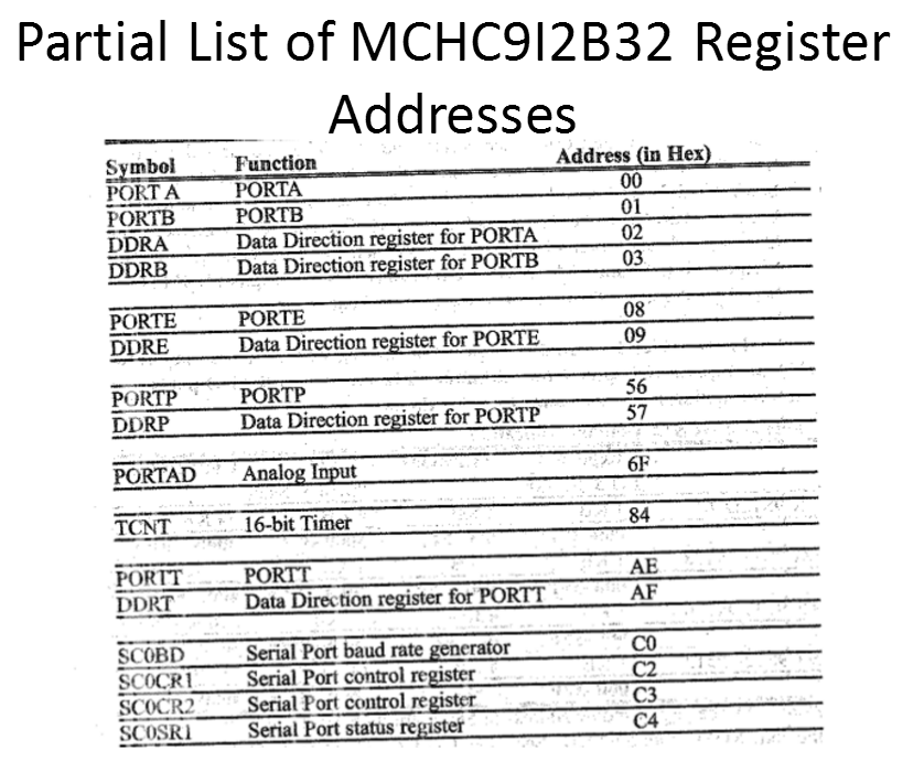
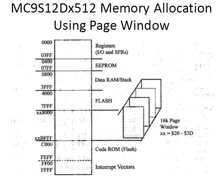
2-2 The HCS12 Memory Map
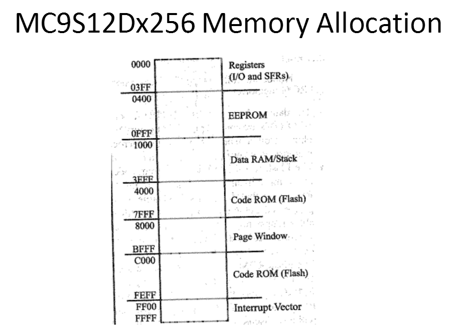
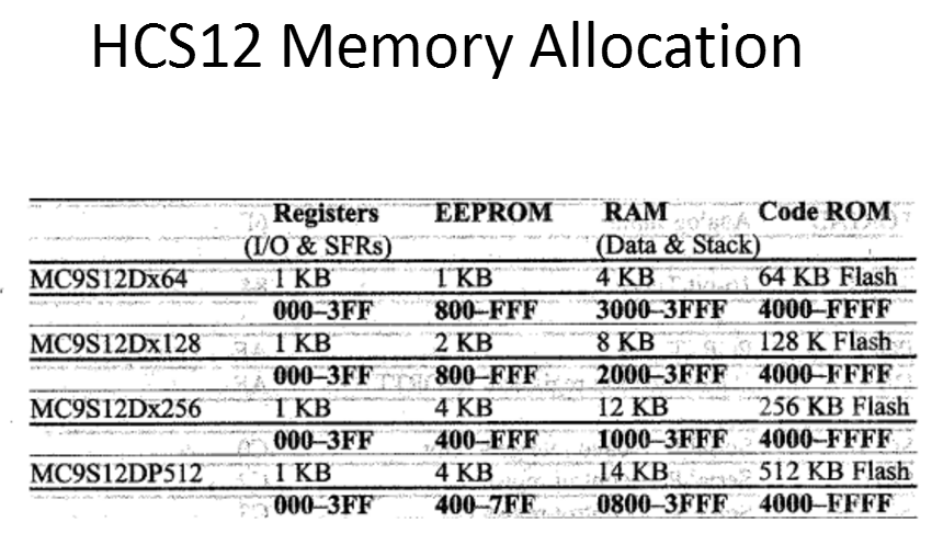
1、Memory Space Allocation in the HCS12
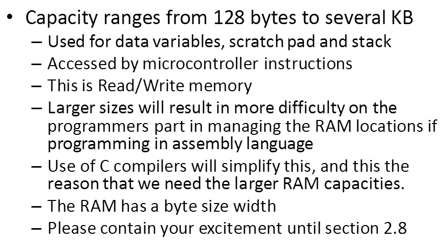
2、Data RAM Space
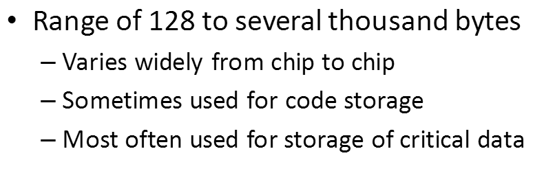
3、EEPROM Space
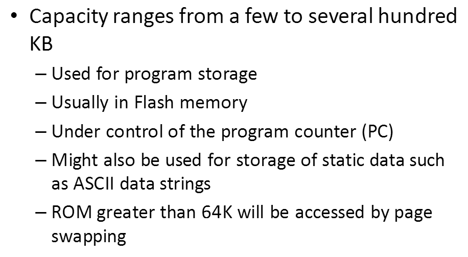
4、Code ROM Space
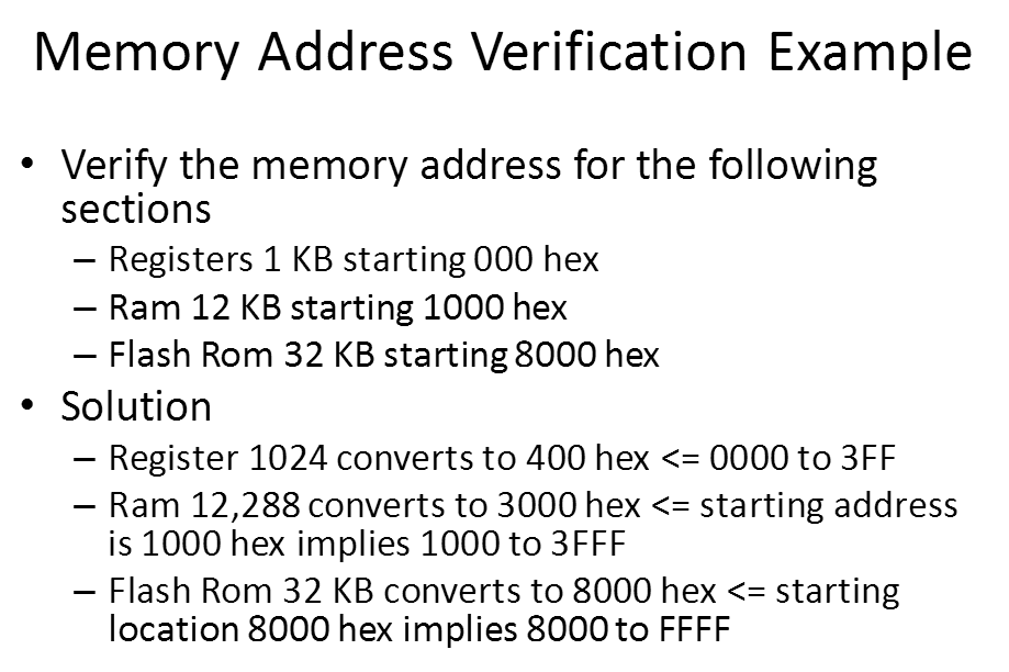
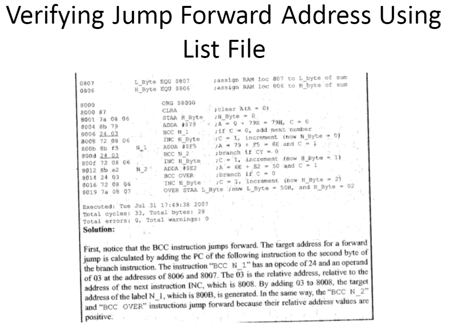
5、Memory Address Verification Example
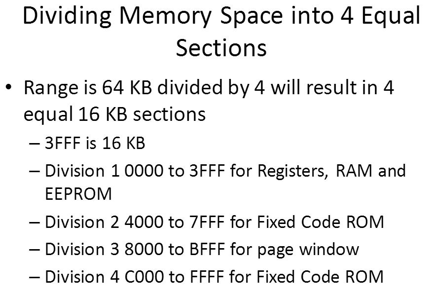
6、Dividing Memory Space into 4 Equal Sections
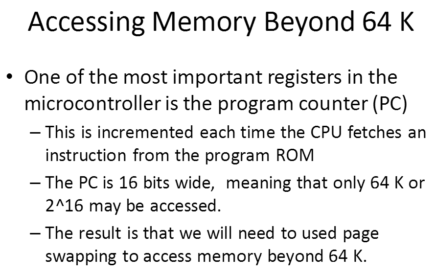
7、Accessing Memory Beyond 64 K
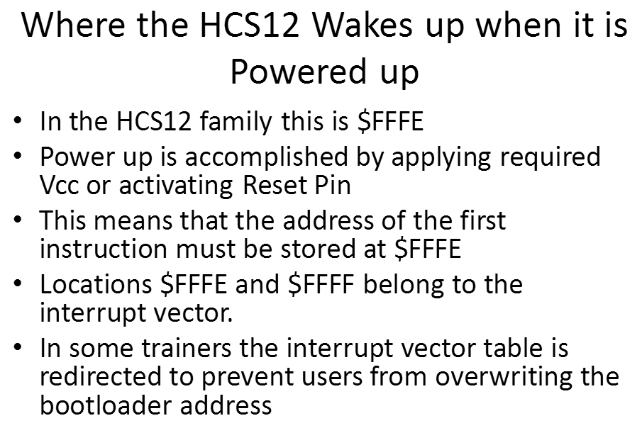
8、Where the HCS12 Wakes up when it is Powered up
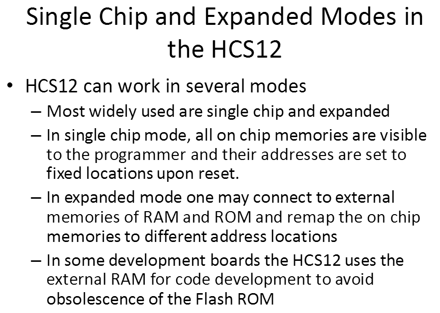
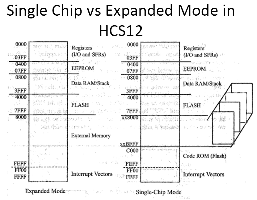
9、Single Chip and Expanded Modes in the HCS12
2-3 HCS12 Addressing Modes
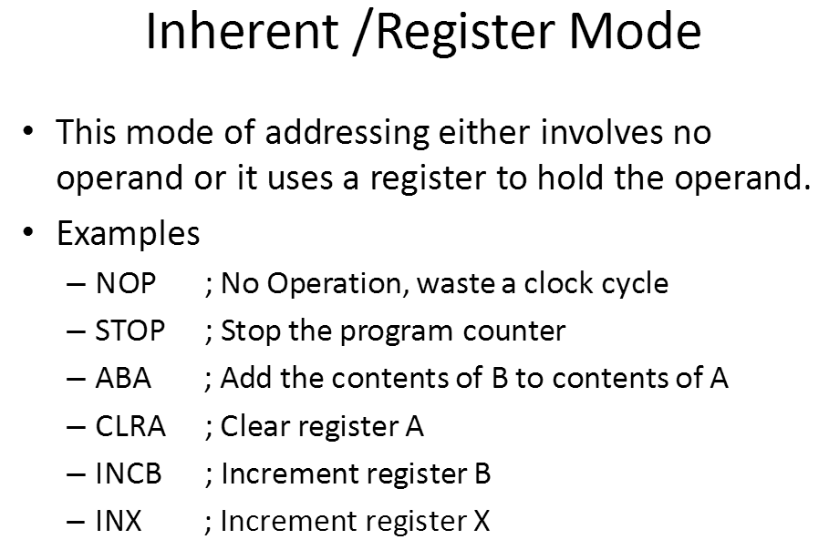
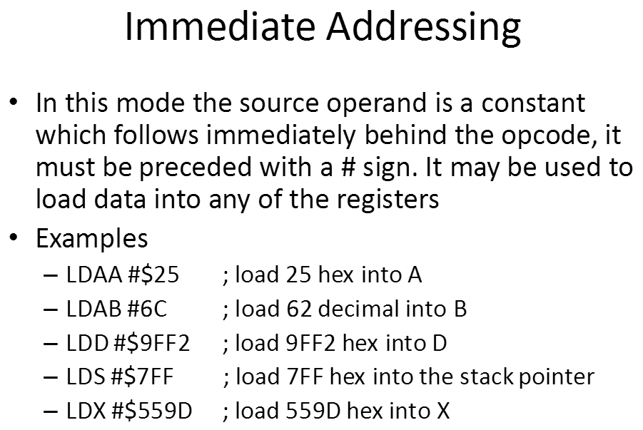
•HCS12 has 6 distinct addressing modes
–Inherent 无操作数
–Immediate 立即数
–Extended 直接访问内存地址
–Direct 直接寻址寄存器
–Relative 间接寻址,多用于跳转
–Indexed 变址寻址,用 X、Y
1、Inherent /Register Mode
2、Immediate Addressing
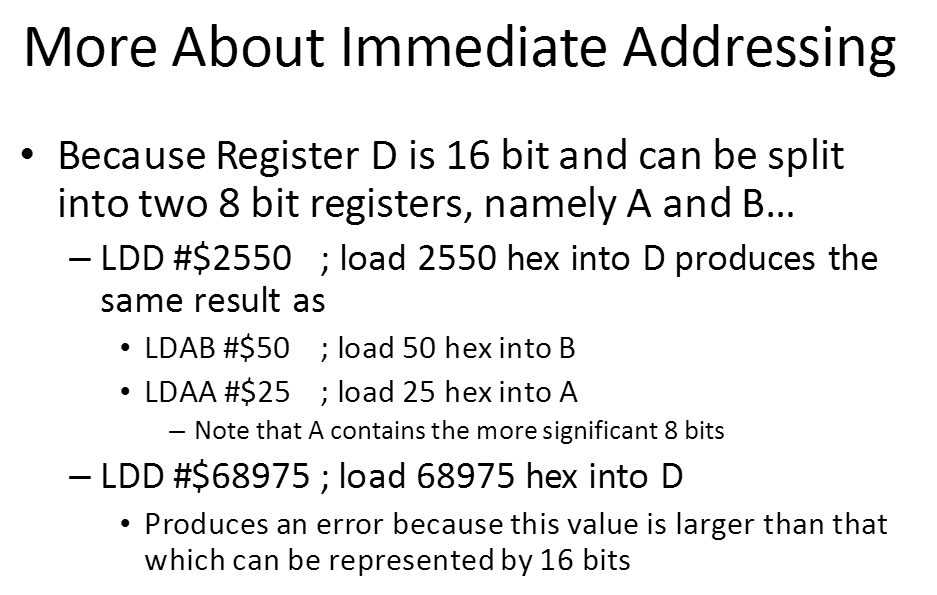
小端是高高低低,这里类似于大端,因为hcs12里面,A地址小于B
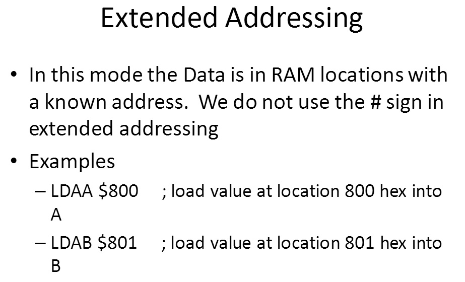
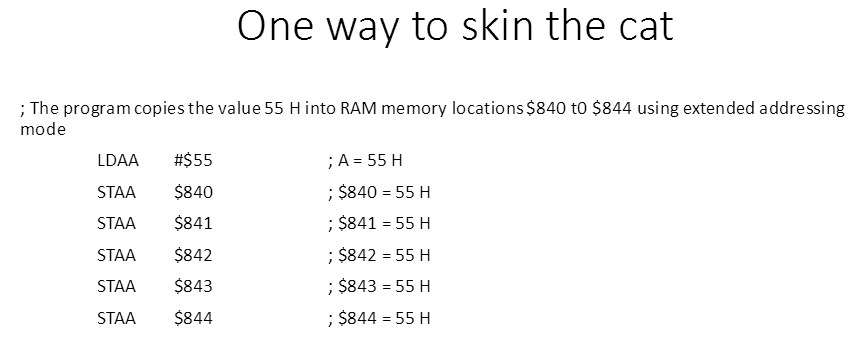
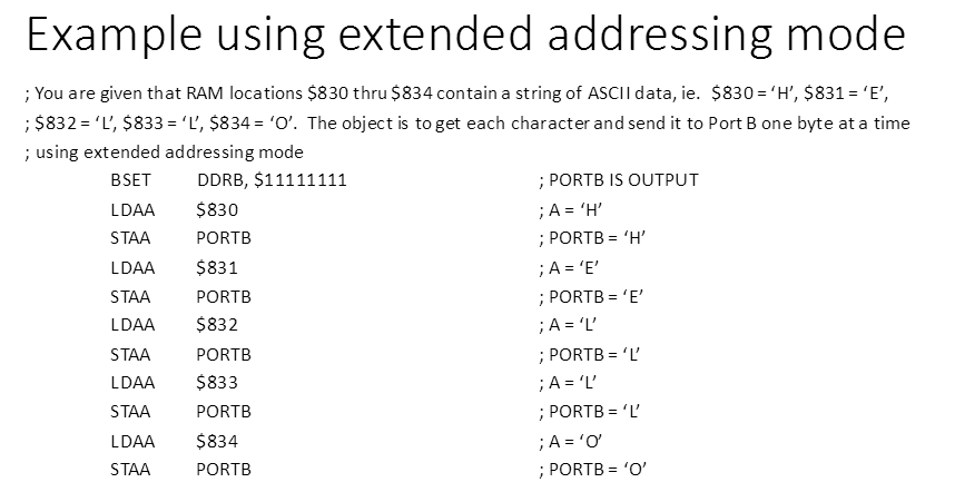
3、Extended Addressing
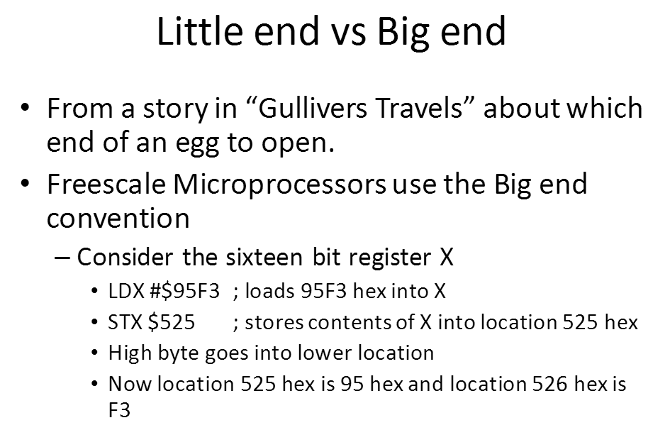
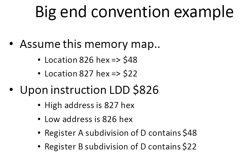
大小端模式
Freescale 微处理器都是大端模式
4、Direct Addressing
特殊的 Extended Addressing,用地址空间寻址寄存器
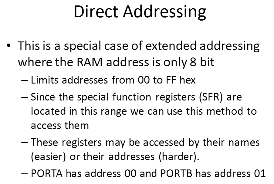
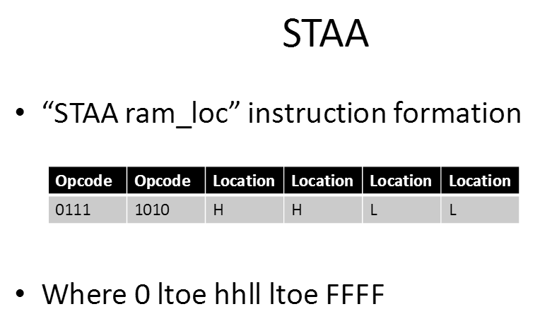
Note the below equivalent methods of storing contents of register A into PORTA
•STAA $00 == •STAA PORTA
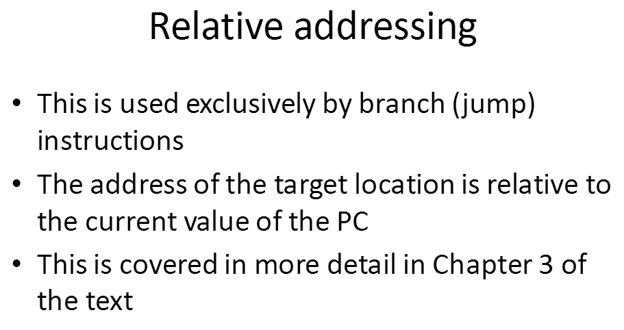
5、Relative addressing 间接寻址,多用于跳转
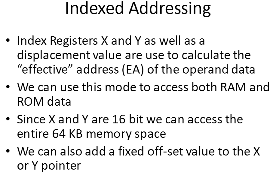
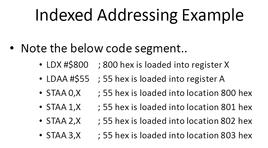
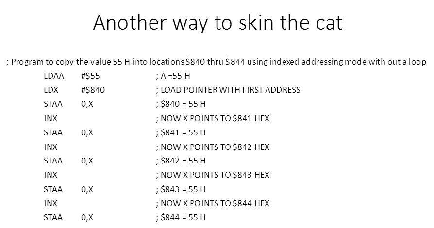
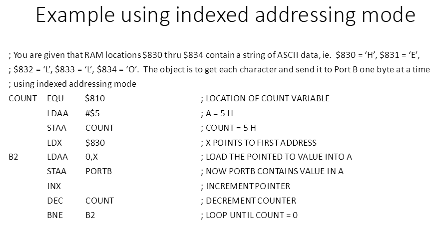
6、Indexed Addressing 变址寻址,用 X、Y
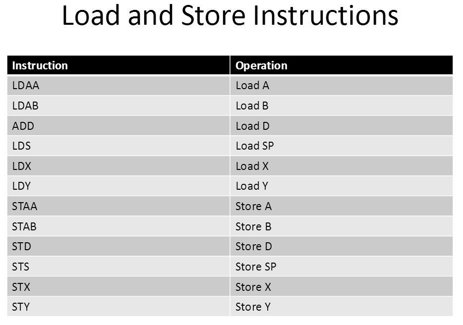
**7、(重要)Load and Store Instructions
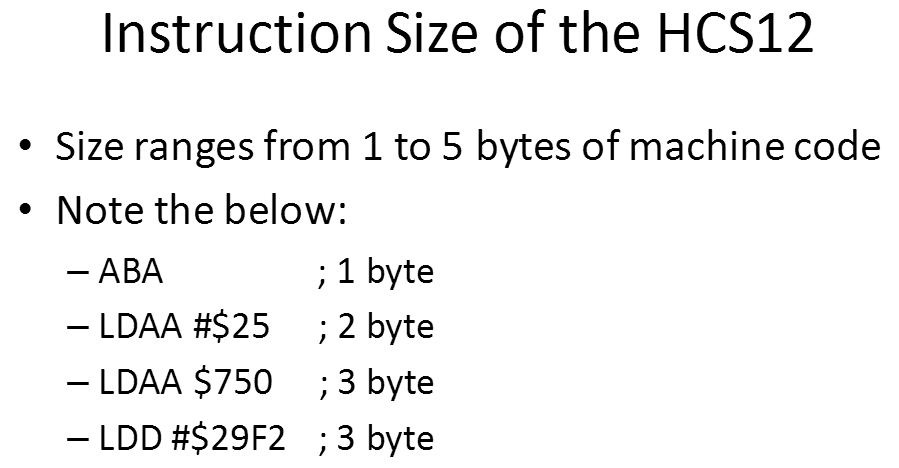
8、Instruction Size of the HCS12
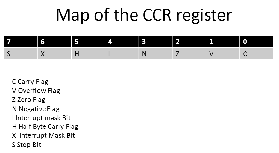
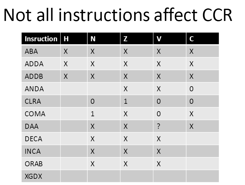
2-4 HCS12 Condition Code Register(CCR)
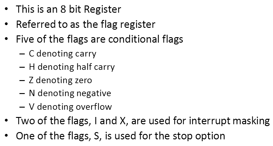
1、C, the carry flag
•Set whenever there is a carry out from the D7 bit
•Affected after 8 or 16 bit addition or subtraction
2、H, the half byte carry flag
•Set when there is carry from D3 bit
•Cleared otherwise
•Used by operations that perform binary coded decimal arithmetic
•Sometimes called the Auxiliary Carry or AC flag
3、Z, the zero flag
•Reflects the result of an arithmetic or logic operation
•Set to 1 for a 0 result
•Set to 0 if result is not zero
•Useful for looping
4、V, the overflow flag
•This flag is set whenever the result of a signed number operation is too large
•The sign bit will therefore be overwritten
5、N, the negative flag
•Bit D7, the MSB in binary representation of 8 bit signed numbers is used to represent sign
–It is 0 for positive numbers and 1 for negative
numbers
•N is 0 when D7 is 0 •N is 1 when D7 is 1
**6、(重要)CCR register
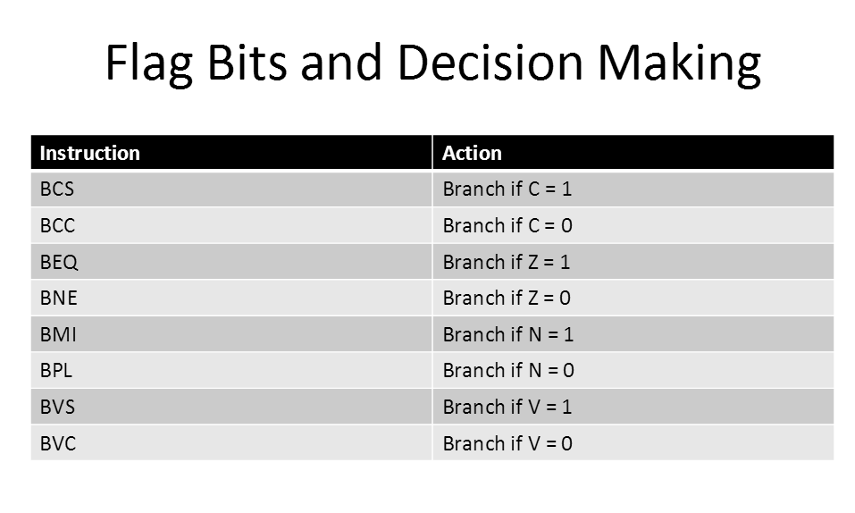
**7、(重要)分支语句(1)CCR基本跳转
2-5 HCS12 Data Format and Directive
4 ways to represent a byte of data in the HCS12 assembler
–Hex
–Binary
–Decimal
–ASCII
1、hex
•Assembly:
–Precede number with $ sign
–Eg. LDDA #$25
•C language
–Precede number with 0x
–Eg. PORTB = 0x99
2、Binary Numbers
•Number is preceded by % sign
–Eg. LDDA #% 00100101 ; 25 hex
3、Decimal Number
•There is no symbol in front of the number
–Eg LDDA #12 ; 0C hex
4、ASCII CHARACTER
•Single quotes around the character are used to denote it as ASCII.
–Eg. LDAA #’9’ loads the value for the character 9
(39 hex)
•Double quotes are used for a string
–Use with the DC (define constant) directive
Assembler Directives
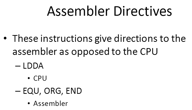
6、EQU
•This is used to define a constant value or fixed address
–Eg. COUNT EQU $25 ; Value of Count defined as 25 hex
–LDDA #COUNT ; Value of register A is 25 hex
SET
•Same as EQU except that:
–Value assigned by the SET directive may be reassigned later
USING EQU for RAM address assignment
•MYCOUNT EQU 5
•MYREG EQU $1200
–LDDA #MYCOUNT
–STAA MYREG ; NOW LOCATION 12OO H IS VALUE 5
Another address example
MYVAL EQU $33
MYRAM EQU $1200 ;RAM ADRESS 1200 H
LDAA #MYVAL ;A = 33H
STAA MYRAM ; STORE A CONTENTS TO 1200 H
STAA MYRAM +1 ; A CONTENT TO 1201 H
STAA MYRAM +2 ; ACONTET TO 1202 H
CLR A ; CLEAR CONTENTS 0F A
ADDA MYRAM ; A=33 H
ADDA MYRAM +1 ; A=66H
ADDA MYRAM +2 ; A=99 H
7、ORIGIN and END DIRECTIVE
•ORG indicates the beginning of the address space
ORG tells the assembler to place the opcode at memory location 0
END DIRECTIVE
•END indicates the end of the source source code.
END indicates the end of the source code to the assembler
8、FCB Directive 可用来定义字符串

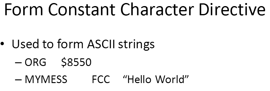
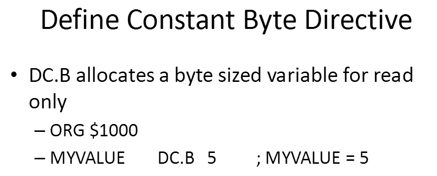
**9、Define Constant Byte Directive 可用来定义字符串
2-6 Introduction to HCS12 Assembly Language
2-7 Assembling and Linking an HCS12 Program
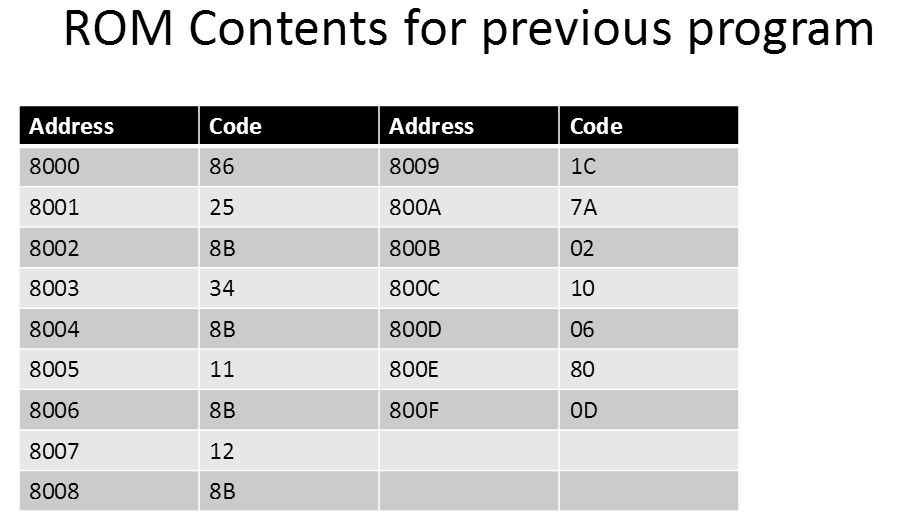
1、链接顺序
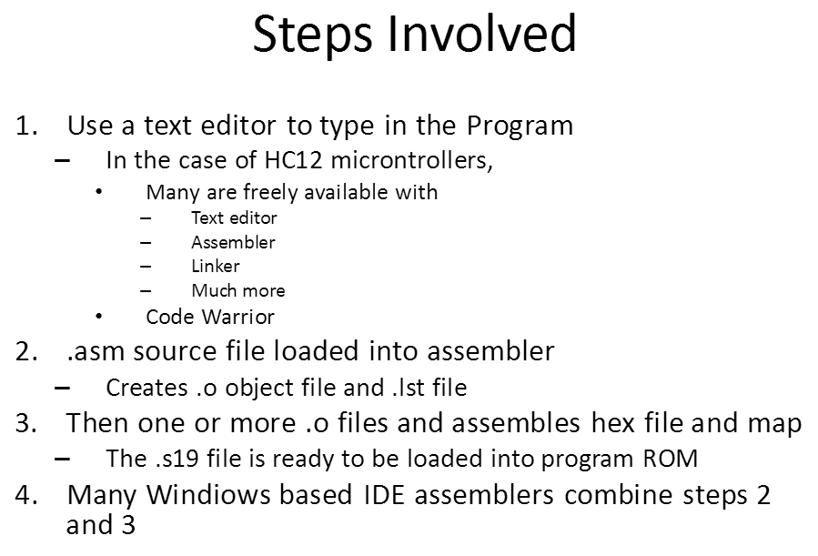
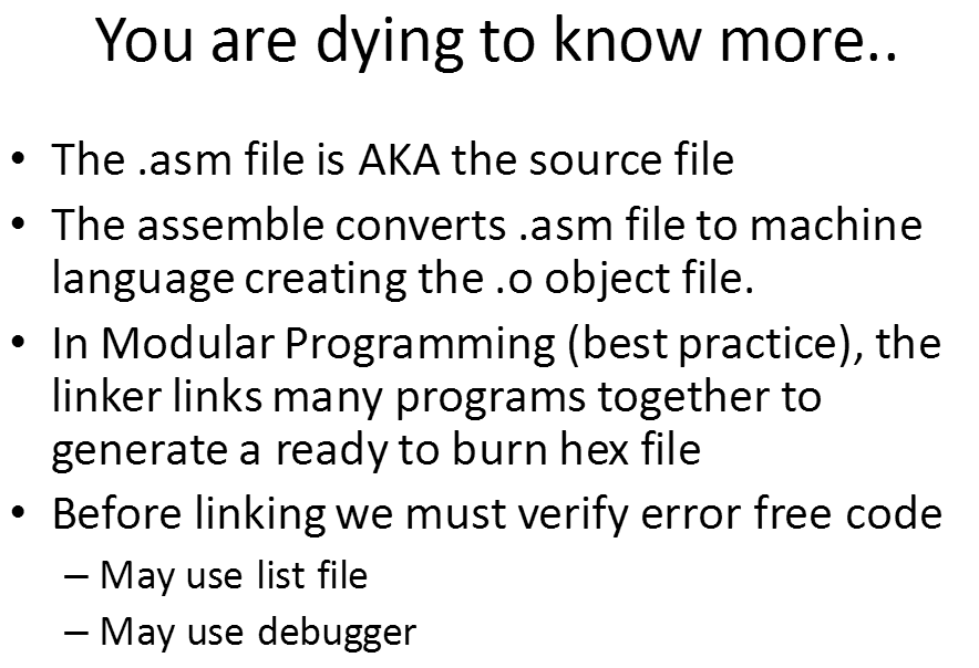
2、例子如下
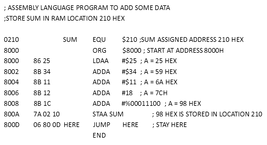
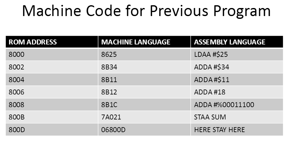
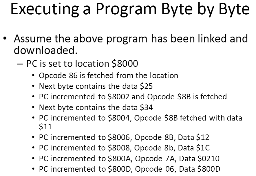
3、Executing a Program Byte by Byte
2-8 Stack and Data Transfer Instructions
1、How Stacks are Accessed in the HCS12
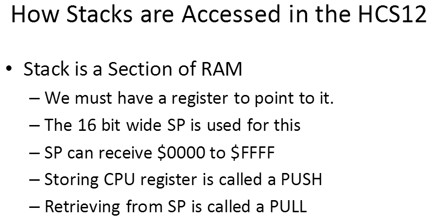
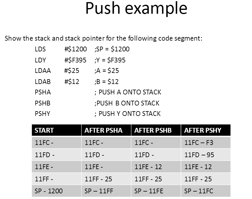
2、Pushing onto the Stack
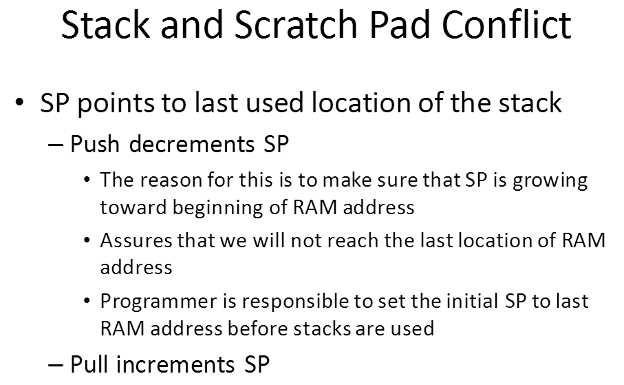
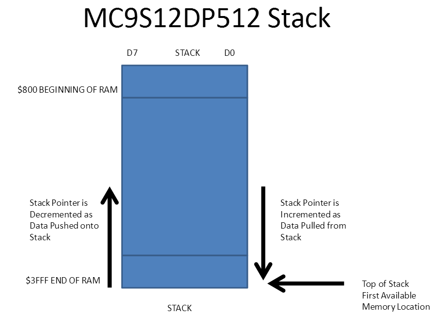
•Stack Pointer points to last used location of the stack
–SP is decremented each time we push
–This is a common convention
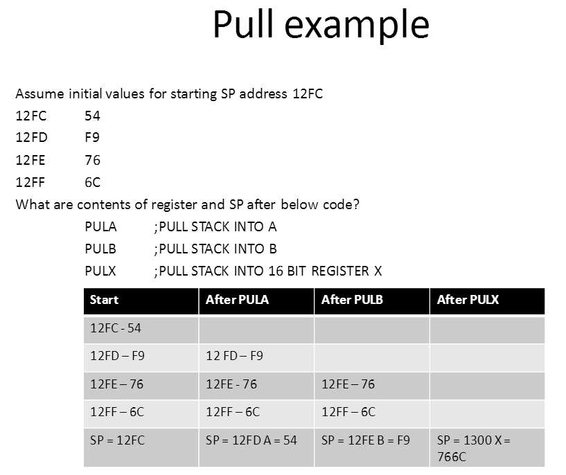
3、Pulling From the Stack
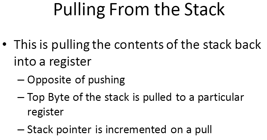
sp在ram最后
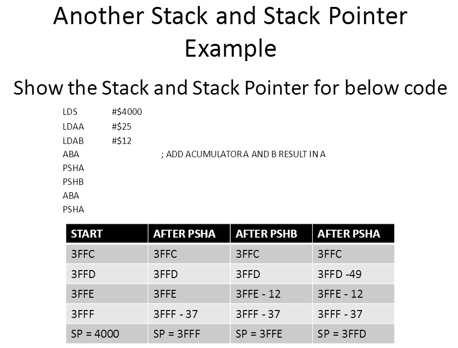
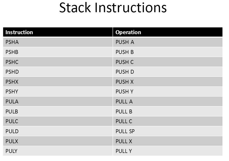
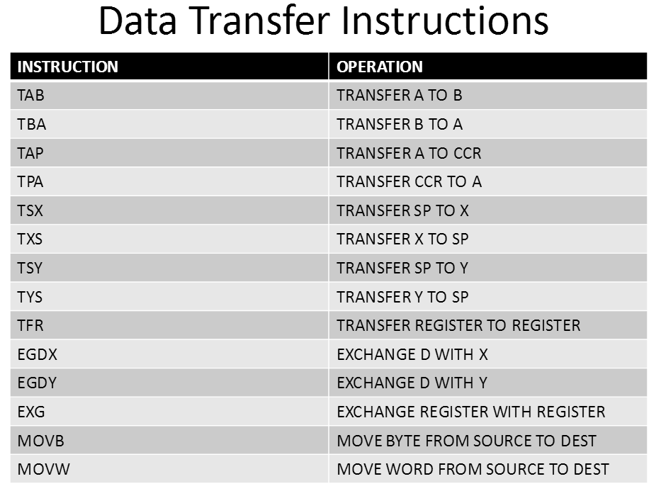
**4、(重要)Stack Instructions & Data Transfer Instructions
Ram area can be thought of as a large number of register
We can rename them as long as we do not use reserved names for SFR’s
三、Chapter 3 Branch, Call and Time Delay Loop
3-1 循环
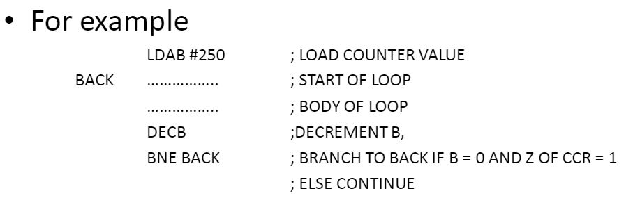
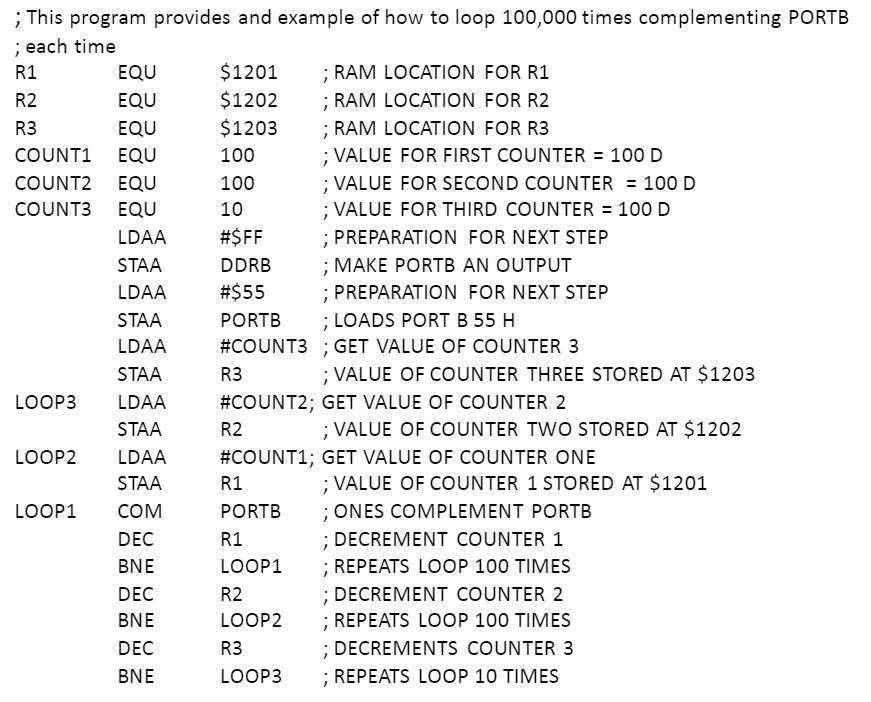
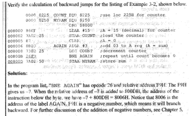
1、Using instruction BNE for Looping
•BNE stands for Branch if Not equal to 0
•For example
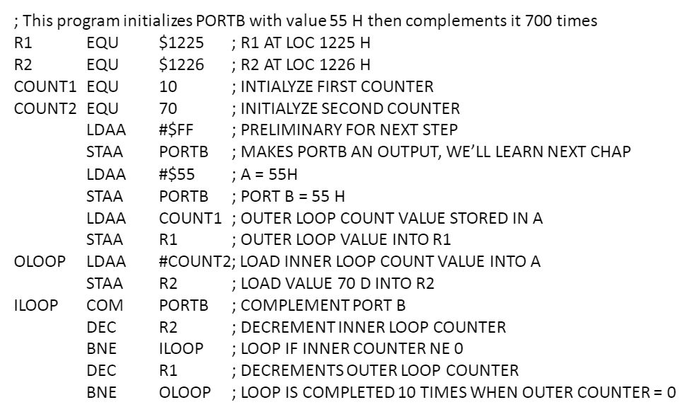
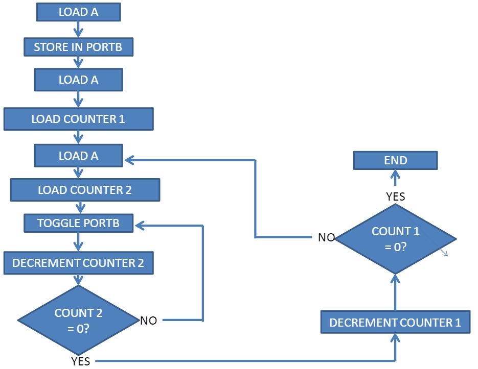
2、Using Ram for Counters
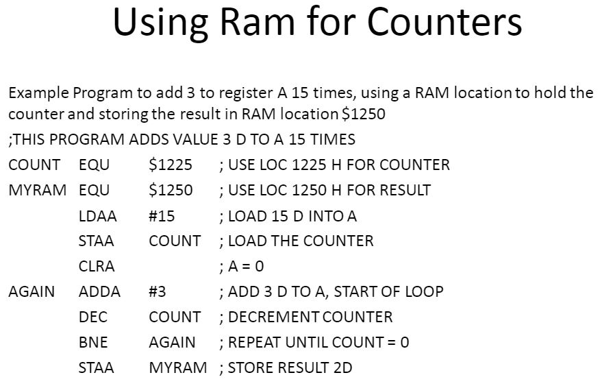
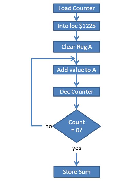
Limitation of previous example
•Because Count is an 8 bit register:
–Maximum of 255 times or FF loops
–One way to overcome this is a nested loop
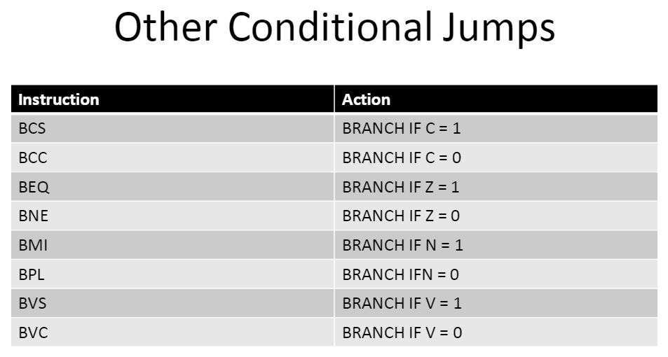
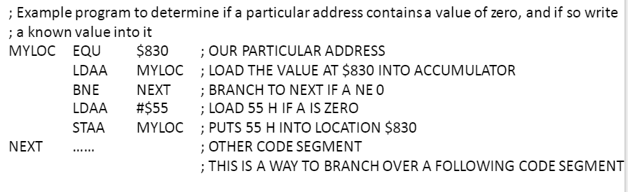
**3、(重要)Other Conditional Jumps
4、Short Conditional Branches
•Target must be within 128 bytes of the contents of PC
•These are 2 bytes instructions
•First byte is opcode
•Second byte is relative address to PC
•Value of second byte may be between -127 and +128
•Jump forward on positive, backwards on negative
•Target address is sum of second byte and PC of next instruction
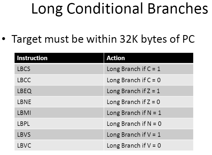
5、Long Conditional Branches
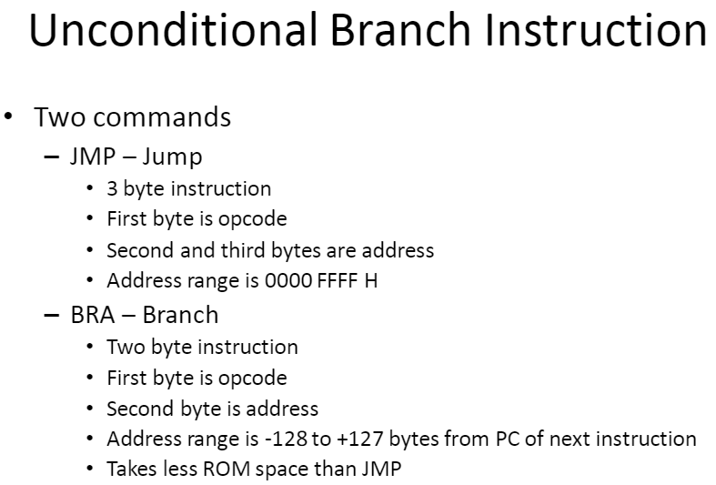
6、Unconditional Branch Instruction
Branching Using the $ Sign
HERE JMP HERE ;EQUIVALENT TO JMP $HERE BRA HERE ;EQUIVALENT TO BRA $3-2 JSR and CALL Instructions
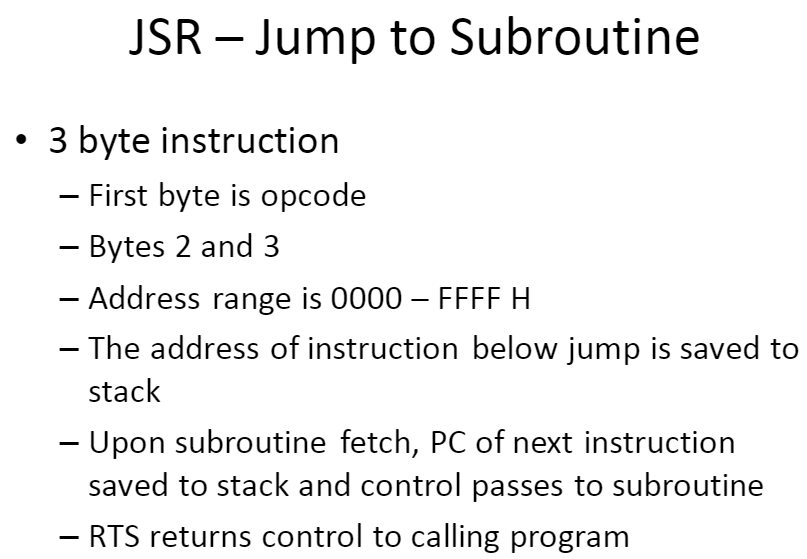
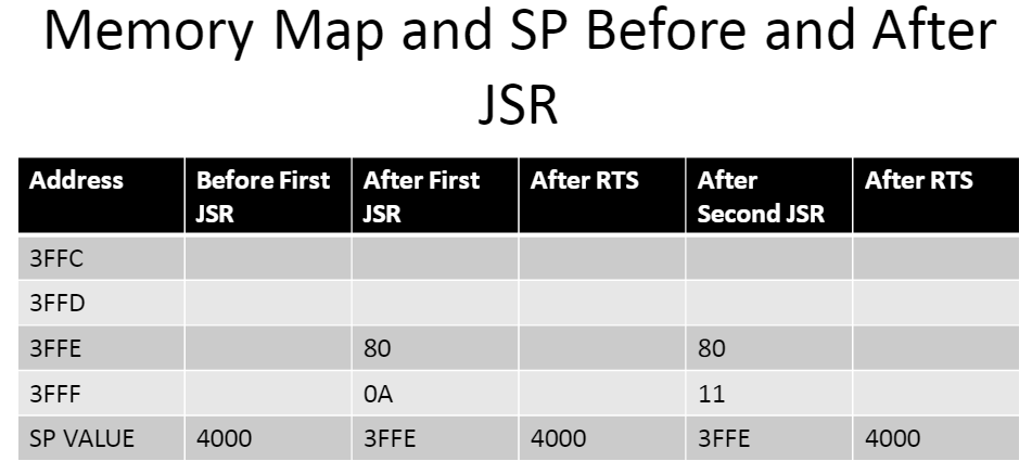
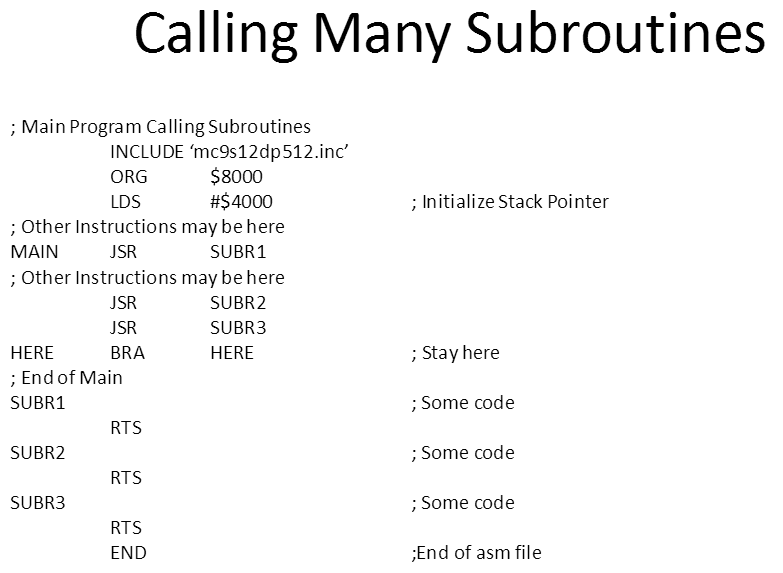
1、JSR – Jump to Subroutine
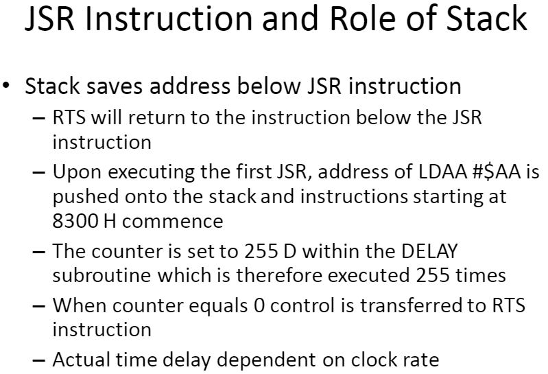
2、JSR Instruction and Role of Stack
Complement A,即 COMA 指令,A 的反码
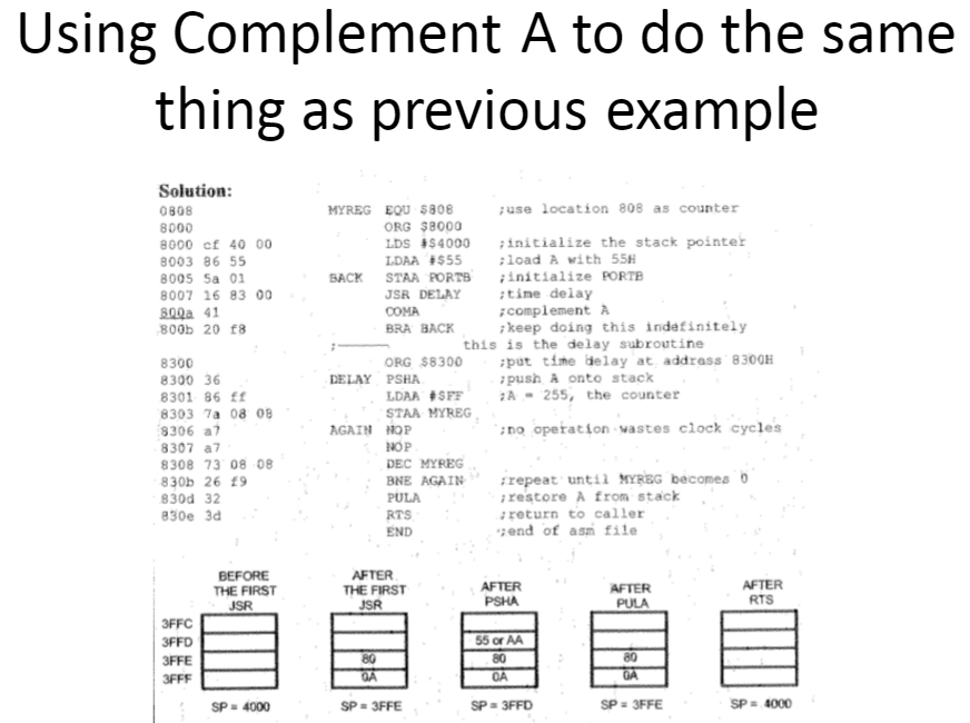
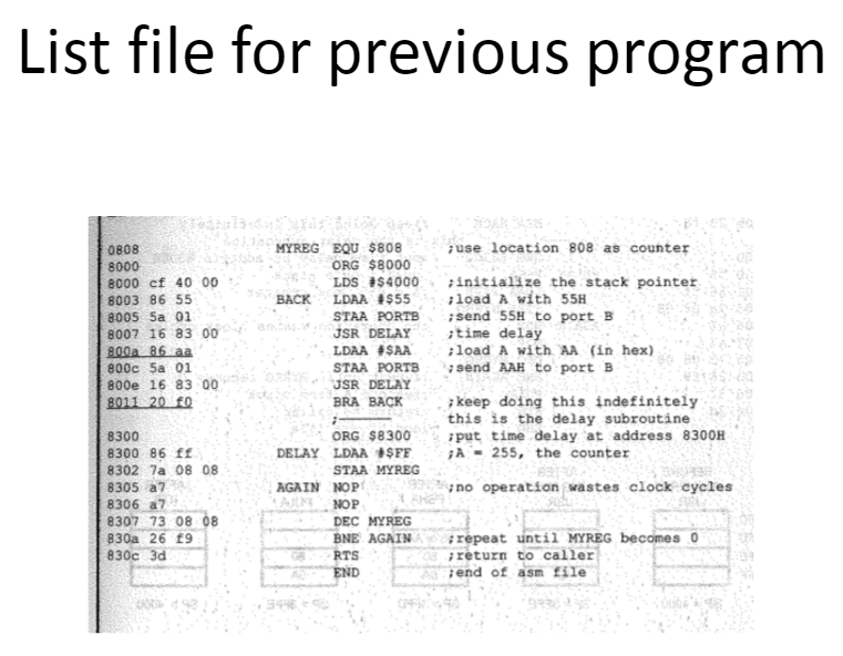
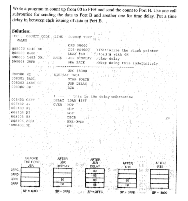
Another List Example
3、Call
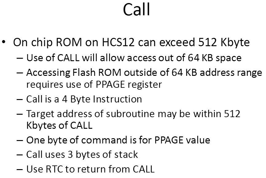
4、CALL vs. JSR
•Assume your particular HCS12 is equipped with 32K on chip Flash ROM.
–Which command would you use?
–JSR is 3 byte instruction and saves ROM
–We do not need to use CALL because we will not go out of 64 KB range
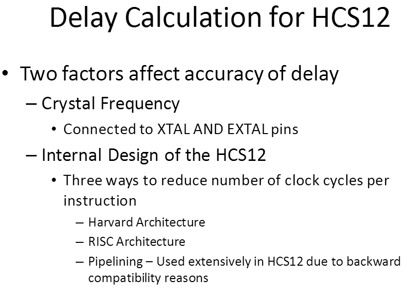
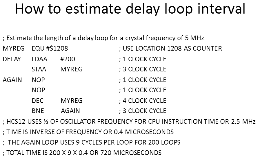
5、Delay Calculation for HCS12
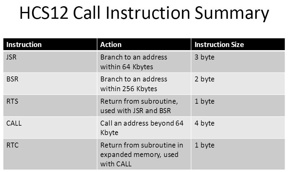
**6、(重要)HCS12 Call Instruction Summary
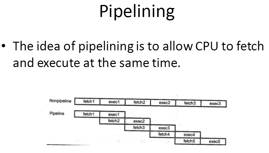
7、Pipelining
8、Instruction Queue and Branch Penalty
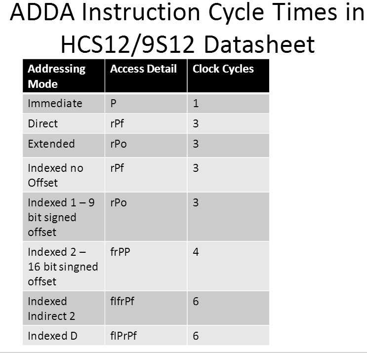
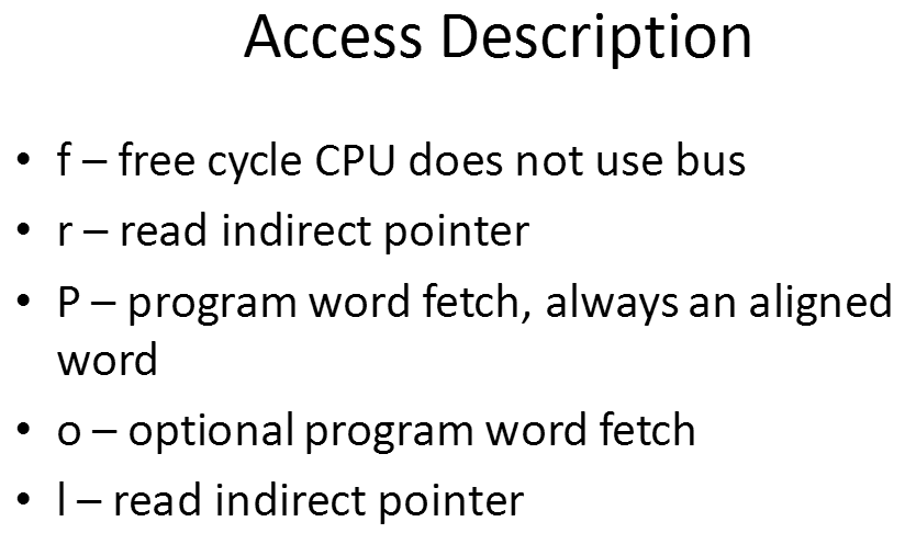
9、Access Description
Bottom Line
•Use timers for more accurate software generated delays
•This is covered in detail in Chapter 9
3-3 Programs Using Indexed Addressing Mode
变址寻址,用X,Y
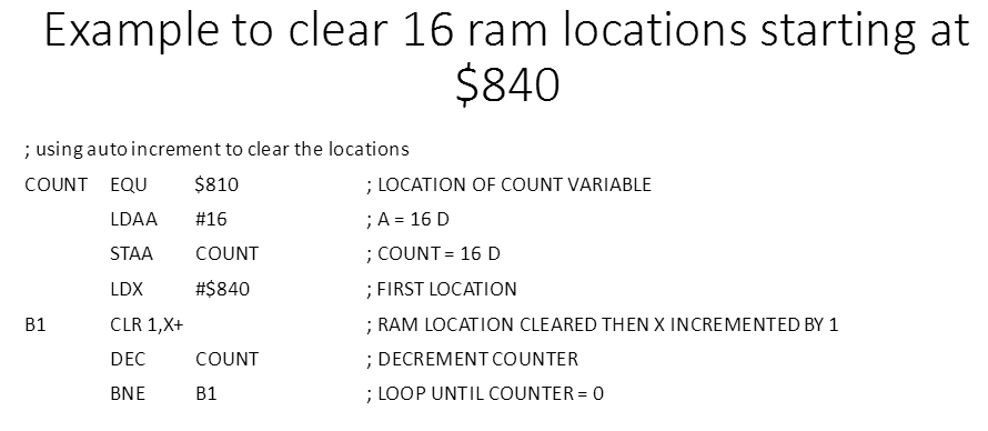
1、Clearing RAM Locations Using a Loop

Clearing Ram Locations with loop 2 bytes at once! Nothing but net

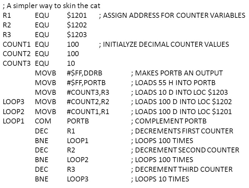
2、Using the MOV Command

MOVB Can Replace Combination of LDAA and STAA


四、Chapter 4 HCS12/9S12 I/O PORT PROGRAMMING
4-1
1、Objectives

2、I/O Ports and their functions
QFP = Quad Flat Package

**3、(重要)Ports in the MC9S12D Family


4、DDR Register and its role in outputting and inputting data
Many of the ports in the 9S12 may be used for either input or output
- DDR register contents determine the Port function at a given point in the program
Writing all 1’s to DDRx configures the Port as an output port and we can subsequently write to the Port itsef
Conversely, writing all 0’s to DDRx configures the Port as an input and we may subsequently read from it.
All ports are configured as input after reset
; code segment to toggle PORTBLDAA #$FF ; A IS ALL ONESSTAA DDRB ; CONFIGURES PORT B AS OUTPUT
L1 LDAA #$55 ; A = 55 HSTAA PORTB ; PORT B IS 0101 0101 B
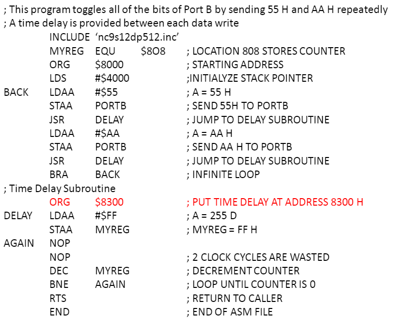
;NOTE THAT COMPLEMENT OF 0101 0101 IS 1010 1010 B OR AA HJSR DELAY ; ZZZZLDAA #$AA ; A = AA HSTAA PORTB ; PORT B IS TOGGLEDJSR DELAY ; ZZZZBRA L1; HERE IS ANOTHER WAY TO SKIN THE TOGGLE PORTB CODEMOVB #$FF,DDRB ; CONFIGURE AS OUTPUT
L1 MOVB #$55,PORTB ; OUTPUT TO PORTBJSR DELAY ; ZZZZMOVB #$AA,PORTB ; OUTPUT COMPLIMENT OF 55 H TO PORTBJSR DELAY ; ZZZZBRA L1 ; TRY IT AGAIN FROM THE TOP
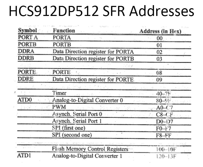
5、Register Addresses for MC9S12DP512 Ports

; PROGRAM TO READ PTH, OPERATE ON IT, THEN STORE RESULT IN PORTBMOVB    #$FF,DDRB  ;PORT B IS OUTPUTMOVB    #00,DDRH    ;PORT H IS INPUT
L2  LDAA    PTH     ; READ FROM PORT HADDA    #5      ; OPERATE ON ITSTAA    PORTB       ; RESULT IN PORTBBRA L2      ; INFINITE LOOP
6、Dual Role of Ports A and B
In expanded mode(直接访问内存地址) the HCS12 uses Port A and Port B for address/data multiplexing allowing connection to external RAM and ROM

7、ERRATA
Port E, and Ports H thru T also have alternative functions and uses in expanded mode.
Analog to digital converter Pins
Depending on the package either 1 or 2, 8 channel ADC’s are available, (122 pin LQFP 2 are available)
We can use the ADC pins for I/O if not used by ADC
4-2 I/O BIT MANIPULATION
1、Bit addressability of I/O Ports(单bit寻址)
Some times it is convenient to access individual bits of Ports and RAM addresses

BSET & BCLR
; PROGRAM TO TOGGLE PB2 AND PB0BSET    DDRB,%00000101  ; THIS MAKES PB2 AN PB0 OUTPUT PINS
AGAIN   BSET    PORTB,%00000101 ; PB2 AND PB0 ARE HIGHJSR DELAY       ; ZZZZBCLR    PORTB,%00000101 ; PB2 AND PB0 ARE LOWJSR DELAY       ; ZZZZBRA AGAIN       ; INFINITE LOOP
2、DUTY CYCLE SQUARE WAVE
; PROGRAM TO CREATE A 50% DUTY CYCLE SQUARE WAVE ON PORTA BIT 0BSET    DDRA,%00000001  ; BIT ZERO IS OUTPUT
HERE    BSET    PORTA,%00000001 ; PA0 IS HIGHJSR DELAY       ; ZZZZBCLR    PORTA,%00000001 ; PA0 IS LOWJSR DELAY       ; ZZZZBRA HERE        ; INFINITE LOOP
; PROGRAM TO CREATE A 66% DUTY CYCLE SQUARE WAVE ON BIT 4 OF PORT ABSET    DDRA,$04   ; DDRA BIT 4 IS OUTPUT
BACK    BSET    PORTA,$04  ; BIT 4 IS HIGHJSR DELAY       ; ONE RINGY DINGYJSR DELAY       ; TWO RINGY DINGIESBCLR    PORTA,$04  ; BIT 4 IS LOWJSR DELAY       ; ONE DELAYBRA BACK        ;  INFINITE LOOP
3、
; PROGRAM TO MONITOR PB2 BIT UNTIL IS BECOMES HIGH THEN WRITE A VALUE TO
; PORT A THEN SEND A HIGH TO LOW PULSE TO PE3BCLR    DDRB,%0000100       ; PB2 IS INTPUTLDAA    #$FF           ; VALUE OF A IS FF HSTAA    DDRA            ; A IS OUTPUTLDAA    #$45           ; VALUE OF A IS 45 H
AGAIN   BRSET   PORTB,%00000100,OVER    ; BRANCH TO OVER IF PB2 IS HIGHBRA AGAIN           ; LOOP UNTIL, MYSTERIOUSLY, PB2; IS LOW
OVER    STAA    PORTA           ; WRITING 45 H TO PORT ABSET    PORTE,%00001000     ; PE3 IS HIGHBCLR    PORTE,%00001000     ; PE3 IS LOW
; ANOTHER WAY TO ACCOMPLISH THE PREVIOUS EXAMPLE USING BRCLR
; INSTRUCTIONBCLR DDRB,%00000100 ; PB2 IS INPUTLDAA #$FF ; A = FF HSTAA DDRA ; PORT A IS OUTPUTBSET DDRE,%00001000 ; PE3 IS OUTPUTLDAA #$45 ; A = 45 H
AGAIN BRCLR PORTB,%00000100,AGAIN ; CHECK IF PB2 IS LOW, IF SO BRANCH; TO AGAINSTAA PORTA ; ELSE WRITE PORT ABSET PORTE,%00001000 ; PE3 IS HIGHBCLR PORTE,%00001000 ; PE3 IS LOW3、monitor
; THINK ABOUT THE APPLICATION OF ALARM MONITORING.  WE COULD USE PB3 AS
; THE BIT THAT MONITORS THIS CONDITION, AND FURTHER ASSUME THAT IT IS
; PULLED LOW WHEN THE DOOR IS OPEN, IT IS A REQUIREMENT TO SEND A HIGH TO
; LOW PULSE TO PE5 TO TURN ON A BUZZERBCLR    DDRB,%00001000      ; PB3 IS INPUTBSET    DDRE,%00100000      ; PE5 IS OUTPUT
HERE    BRSET   PORTB,%00001000,HERE    ; BRANCH IF PB3 IS HIGH TO HEREBSET    PORTE,%00100000     ; PE5 IS HIGHBCLR    PORTE,%00100000     ; PE5 IS LOW
附加:
1、Branch instructions for Signed numbers
2、Show how the cpu would subtract $05 from $43.
这个时候需要考虑到补码,43H-05H=3EH,也就是0100 0011 - 0000 0101,这个时候减去这个数相当于加上这个数的反码,0100 0011 + 1111 1011 = 0011 1110
五、Chapter 5 Arithmetic, Logic Instructions and Programs
5-1
1、Learning Objectives
Upon completion, Students will be able to:
Define the range of numbers in HCS12 for unsigned data
Code addition and subtraction of numbers for unsigned numbers
Perform addition of BCD data
Code HCS12 multiplication a division of unsigned numbers
Code HCS12 logic instructions: AND, OR, and EX-OR
Code HCS12 assembly instructions for bit shift and rotate
Use HCS12 logic instructions for bit manipulation
Use Compare for program control
Code HCS12 rotate instructions and data serialization
Explain BCD system of data representation
Contrast and compare packed and unpacked BCD data
Code HCS12 programs for ASCII and BCD data conversion
Define the range of numbers possible in HCS12 for signed data
2、Example using ADCA(带carry的加)
; Program to add two 16 bit numbers using ADCA instruction.  The numbers are 3CE7
; H and 3B8D H.  Assume big endian convention, and 3B8D are stored in locations 807
; and 806.  The result is stored in locations 808 and 809LDAA    #$E7       ; A = VALUE OF FIRST NUMBER LOW BYTEADDA    $807       ; LOCATION OF NEXT LOW BYTE ; E7 + 8D = 174 AND C = 1STAA    $809       ; STORE ACCORDING TO CONVENTIONLDAA    #$3C       ; A = VALUE OF FIRST NUMBER HIGH BYTEADCA    $806       ; A = A + VALUE OF NEXT HIGH BYTE + 1STAA    $808       ; STORE RESULTANT HIGH BYTE BIG ENDIAN
3、Adding Multi-Byte Numbers
; Program to add two multi-byte numbers
MYCOUNT EQU $800       ; ADDRESS OF COUNTER VARIABLELDAA    #4      ; A = 4 DSTAA    MYCOUNT ; VALUE OF MYCOUNT IS 4 DCLRA            ; A = 0LDX #$813      ; X POINTERLDY #$853      ; Y POINTERCLC         ; CLEAR CARRY FLAG
BACK        LDAA    0,X     ; LOAD BYTE AT POINTED ADDRESSADCA    0,Y     ; ADD BYTE AT POINTED ADDRESSSTAA    0,Y     ; STORE WITH CARRYDEX         ; DECREMENT POINTER XDEY         ; DECREMENT POINTER YDEC MYCOUNT ; DECREMENT LOOP COUNTERBNE BACK        ; BRANCH IF COUNTER NE 0
4、DAA Instruction
DAA stands for Decimal Adjust Accuumulator
- Only works with A register
- Adds 6 to lower nibble and higher nibble if necessary, otherwise no effect
Consider the following
LDAA    #$47		; A = $47
ADDA    #$25       ; A = A + 25 H  RESULT IS 6C H
DAA             ; ADUST FOR BCD ADDITION, RESULT IS 72 H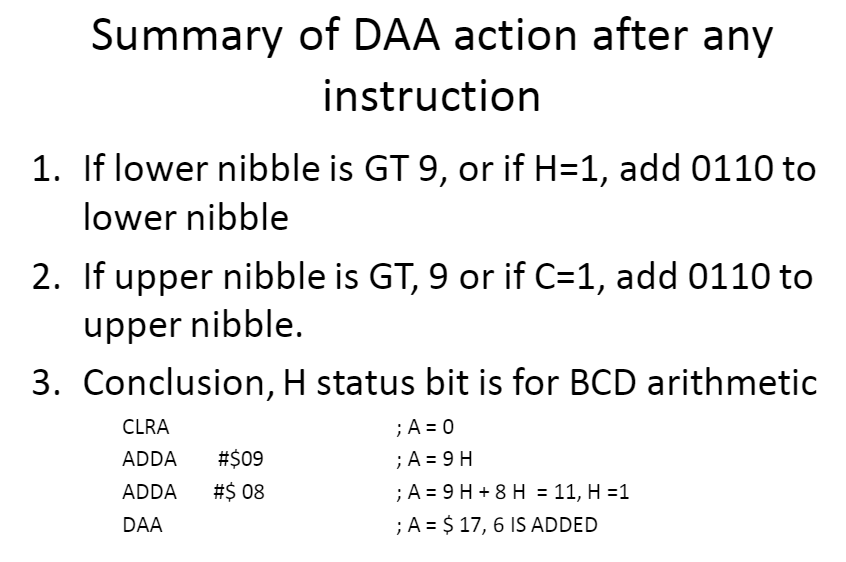
5、Subtraction of unsigned numbers

6、Neg Instruction
- After execution of SUBA, if C = 0 the result is positive
If C = 1, the result is negative - Destination has 2’s complement of result
- NEG (negate) may be used to change this
- NEG performs 2’s complement

; Program to subtract 6E H from 4C H
MYREG   EQU $820       ; LOCATION OF NUMBER TO BE SUBTRACTEDLDAA    #$6E       ; A = 6E HSTAA    MYREG       ; STORE 6E H AT LOCATION 820 HLDDA    #$4C       ; A = 4C HSUBA    MYREG       ; A = (4C-6E) = DE, INVERTED C = 1BCC NEXT        ; IF C = 0 BRANCH TO NEXT TARGETNEGA            ; TAKE 2’S COMPLEMENT OF A
NEXT    STAA    MYREG       ; RESULT IS STORED IN MYREG
; 6E = 01101110 2’S COMPLIMENT OF THIS IS 1001 0010
; AFTER THE SUBA COMMAND C =1 AND THE RESULT IS NEGATIVE WE DO NOT
; BRANCH AND 2’S COMPLEMENT IS TAKEN AND MYREG = 22 H MAGNITUDE OF
; NEGATIVE RESULT
7、SBCA SUBTRACT WITH BORROW
- Used for multi-byte numbers
- Handles borrow of lower byte
- C flag holds borrow
- If C = 1 prior to execution, 1 is subtracted from result
; Program to subtract 2 16 bit numbers eg $2762 - $1296 assuming location 806 H
; stores 12 H and location 807 H stores 96 H, store result in same locations with big
; endian convention.  We  are looking for the result of 14CCLDAA    #$62       ; LOAD LOW BYTESUBA    $807       ; A = 62 H – 96 H = CC H, C = BORROW = 1STAA    $807       ; STORE LOW BYTELDAA    #$27       ; LOAD HIGH BYTESBCA    $806       ; A = 27 – 12 – 1 = 14 HSTAA    $806       ; STORE HIGH BYTE
; Since these are 16 bit or 2 byte numbers, we could us the instruction SUBDLDD #2762       ; LOAD D REGISTERSUBD    $806		; SUBTRACT THE VALUES AT $806 AND $807STDD    $806       ; STORE RESULT
**8、(重要)Some Widely Used Arithmetic Instructions

9、Multiplication of unsigned numbers

; Multiply 25 H by 65 HLDAA    #$25       ; FIRST OPERAND IN ALDAB    #$65       ; SECOND OPERAND IN BMUL         ; 25 H x 65 H = E99 H IN REG D; A = 0E H, B = 99 H
;
; 16 bit multiplicationLDD #500        ; D = 500 DECIMALLDY #700        ; Y = 700 DECIMALEMUL            ; 500 x 700 = 350000 = 55730 H; Y = 0005 H, D = 5730 H
10、Unsigned Multiplication and Division Summary

11、Unsigned Division
; divide 255 decimal by 10 decimalLDD #255        ; D = 255 DECIMALLDX #10     ; X = 10 DECIMALIDIV            ; 255/10 = 25 REMAINDER 5
`               ; X = 25 DECIMAL AND D = 5
;
; divide 90FF24 H by 1000 decimal
;LDD #$FF24     ; LOWER WORDLDY #$90       ; UPPER WORD; 90FF24 H = 9502500 DECIMALLDX #1000       ; X = 1000 DECIMALEDIV            ; Y:D/X = 9502 (251E H) REMAINDER 500 (1F4)
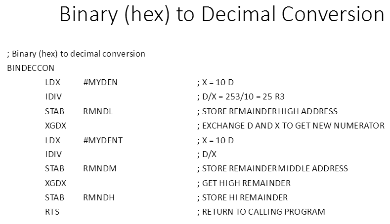
Division Application Example ADC
; ADC provides Hex data between 00 and FF H. Conversion to decimal is accomplished
; by dividing by 10 repetitively and saving remainder. This program converts FD H to
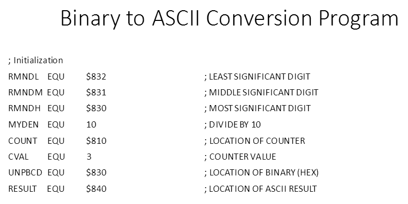
; decimal with byte by byte division using locations 822 – 824 H to store results where 824 is LSD
RMNDL EQU $824 ; LOCATION OF LEAST SIGNIFICANT DIGIT
RMNDM EQU $823 ; LOCATION OF MIDDLE SIGNIFICANT DIGIT
RMNDH EQU $822 ; LOCATION OF HIGH SIGNIFICANT DIGIT
MYNUM EQU $FD ; FD H = 253 D
MYDEN EQU 10 ; DENOMINATOR IS 10 DECIMALORG $8000 ; START AT 8000 HLDD #MYNUM ; LOAD NUMERATOR IN REGISTER DLDX #MYDEN ; LOAD DENOMINATOR IN REGISTER XIDIV ; 253/10 = 25 R 3STAB RMNDL ; SAVE REMAINDER ALWAYS LT 10, 3 IN THIS CASEXGDX ; EXCHANGE D AND X FOR NEW NUMERATOR 25LDX #MYDEN ; X = 10IDIV ; 25/10 = 2 R 5STAB RMNDM ; SAVE NEXT DIGIT, 5 IN THIS CASEXGDX ; X IS NOW 5 AND D IS 2STAB RMNDH ; STORE FINAL DIGIT 25-2 Logic Instructions and Programs 逻辑运算
1、Some Widely Used Boolean Logic Instructions in HCS12
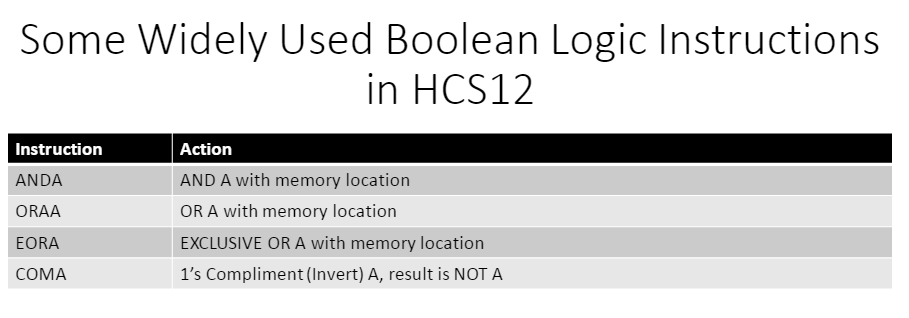
NEG 是2的补码
2、Using XOR to toggle bits of operand
    LDAA        #$FFEORA        PORTB       ; ALL BITS ARE CHANGEDSTAA        PORTB       ; TO OPPOSITE VALUE
;   $FF    1111 1111
; XOR   $45    0100 0101           ; ASSUMED VALUE
;       1011 1010
;   $BA
; COULD WE DO THIS WITH COM INSTRUCTION?
3、Negate command NEG

4、BRSET Instruction
- Branch if certain bits set high
- Mask Byte indicates bits to check
- BRSET performs AND on mask byte and inverted memory location
– The branches if all bits are 0
; Given that PB7 is used to monitor the status of a switch, write a program to toggle PA0 when ever the switch
; goes high.  Then further analyze the cases of PB7 = 1 and PB7 = 0BCLR    DDRB, %10000000     ; PB7 IS INPUTBSET    DDRA, %00000001     ; PA0 IS OUTPUT
BACK    BRSET   PORTB, %10000000    , TOG   ; BRANCH TO TOG IF PB7 IS HIGHBRA BACK            ; KEEP CHECKING IT
TOG BCLR    PORTA, %00000001        ; PA0 = 0BSET    PORTA, %00000001        ;PA0 = 1BRA BACK            ; CHECK PB7 AGAIN
; CASE 1 PB7 = 1    MASK BYTE   1000 0000
; AND INVERTED PORTB        0000 0000
; RESULT            0000 0000   IT WILL BRANCH
; CASE 2 PB7 = 0    MASK BYTE   1000 0000
; AND INVERTED PORTB        1000 0000
; RESULT            1000 0000   IT WILL NOT BRANCH
5、BRCLR Instruction
- Branch if clear branches if certain bits of target are low. .
- Mask byte indicates the bits to be checked
- The instruction performs a logical and between the mask byte and the target location and branches if all bits are low.
; You are given that PB2 is used to monitor the status of a switch.  Write a program to toggle PA7 whenever
; PB is low.  Further analyze each of the two possible cases.BCLR    DDRB, %00000100         ; PB2 IS INPUTBSET    DDRA, %10000000         ; PA7 IS OUTPUT
BACK    BRCLR   PORTB, %00000100, TOG       ; BRANCH TO TOG IF PB2 = 0BRA BACK                ; KEEP LOOKING AT PB2
TOG BCLR    PORTA, %10000000            ; PA7 = 0BSET    PORTA, %10000000            ; PA7 = 1BRA BACK                ; KEEP LOOKING AT PB2
; CASE 1 PB2 = 1    MASK BYTE   00000100
; AND       PB2 00000100
; RESULT            00000100    WILL NOT BRANCH
; CASE 2 PB2 = 0    MASK BYTE   00000100
; AND       PB2 00000000
; RESULT            00000000    WILL BRANCH
5-3 Compare Instruction and Programs
1、Compare instructions
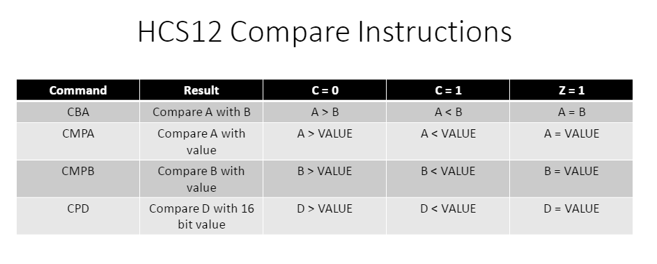
本质是相减比较大小
; Program determines if data on PORTB contains the value 99 H, If so, write ‘Y’ to Port A else write ‘N’ to Porta.BCLR    DDRB, %11111111         ; PORT B IS INPUTBSET    DDRA, %11111111         ; PORT A IS OUTPUTLDAA    #’N’                ; A IS ASCII NSTAA    PORTA               ; PORT A IS ‘N’LDAA    #$99               ; A IS 99H
BACK    COMPA   PORTB               ; IS PORTB = 99 H?BNE BACK                ; NO KEEP CHECKINGLDAA    #’Y’                ; YES WRITE TO PORT ASTAA    PORTA               ; PORT A IS ‘Y’
; PROGRAM FINDS THE GREATER OF TWO VALUES AND PLACES THE LARGER ONE IN LOCATION $820
VAL1    EQU 54          ; 54 D
VAL2    EQU 27          ; 27 D
BIG EQU $820           ; VARIABLE ASSIGNED TO LOCATIONLDAA    #VAL1           ; A = 54 DCMPA    #VAL2           ; COMPARE 54 D TO 27 DBCS OVER            ; JUMP IF VAL1 < VAL2 (C = 1)STAA    BIG         ; VAL1 > VAL2, STORE A INTO BIG
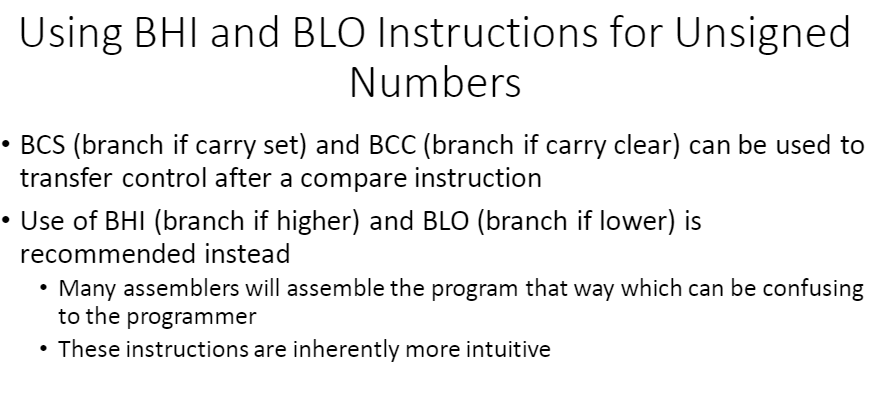
2、Using BHI and BLO Instructions for Unsigned Numbers
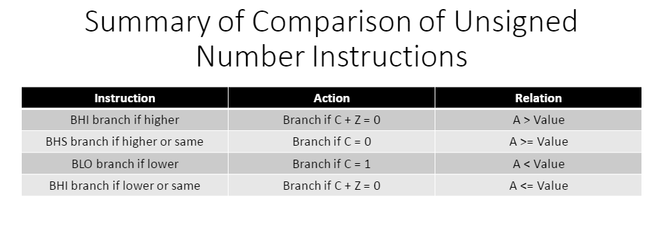
3、Summary of Comparison of Unsigned Number Instructions
5-4 Rotate, Shift Instructions and Data Serialization
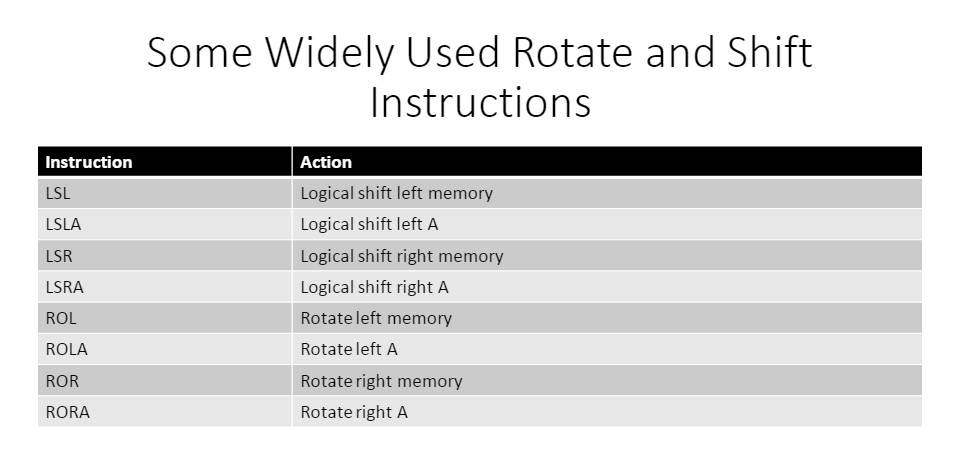
1、Some Widely Used Rotate and Shift Instructions
2、Serializing Data

3、Program to find the number of ones
; Program to find the number of ones in a given byte
R1  EQU $820           ; LOCATION OF VARIABLE TO STORE NUMBER OF 1’S
COUNT   EQU $821           ; LOCATION OF COUNT VARIABLE
VALUE   EQU $822           ; LOCATION OF DATA BYTECLC             ; C = 0CLRA                ; A = 0STAA    R1          ; INITIAL R1 VALUE IS 0LDAA    #8          ; A = 8 DSTAA    COUNT           ; INTIALYZE COUNTER TO 8 DLDAA    #$97           ; WE WILL FIND THE NUMBER OF 1’S IN 97 H OR 1001 0111 BSTAA    VALUE           ; DATA BYTE INITIALYZED
AGAIN   ROLA                ; ROTATE LEFT THRUOU CARRYBCC NEXT            ; IF C = 0 BRANCH TO NEXTINC R1          ; ELSE INCREMENT THE NUMBER OF 1’S
NEXT    DEC COUNT           ; DECREMENT COUNTERBNE AGAIN           ; GET NEXT BIT FOR 8 TIMES
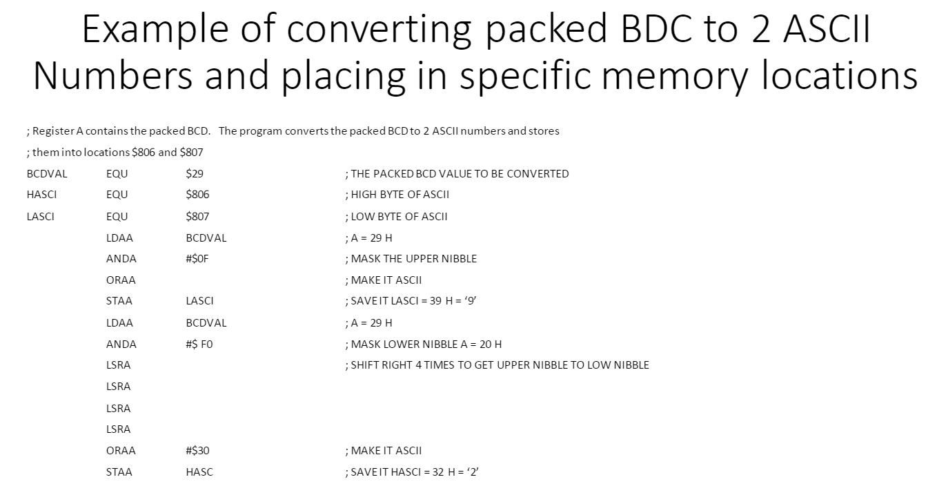
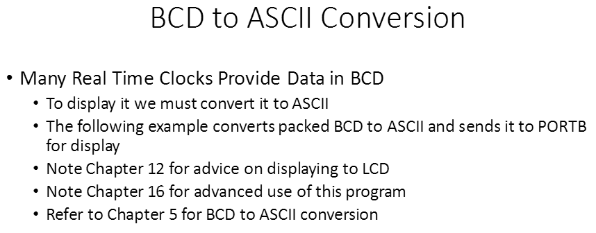
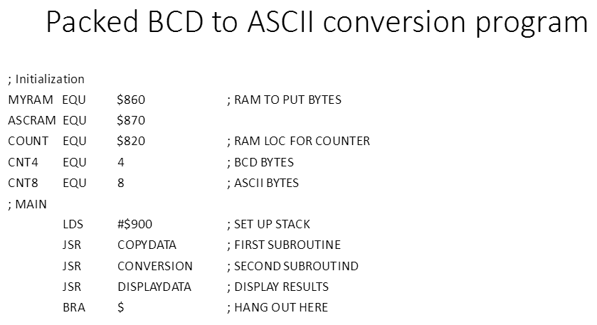
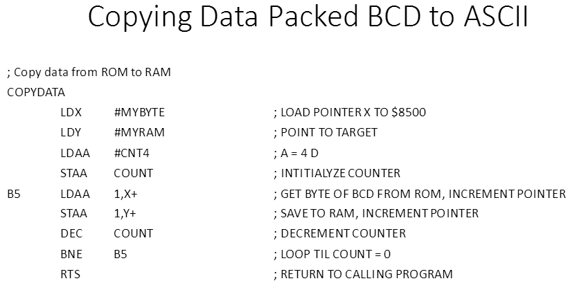
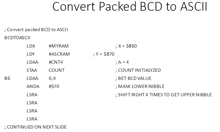
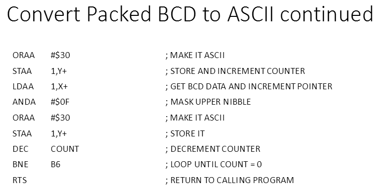
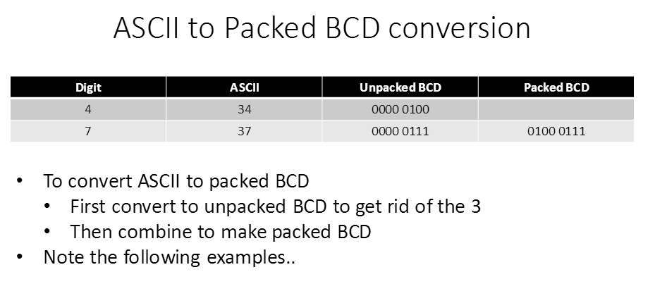
5-5 BCD and ASCII Conversion
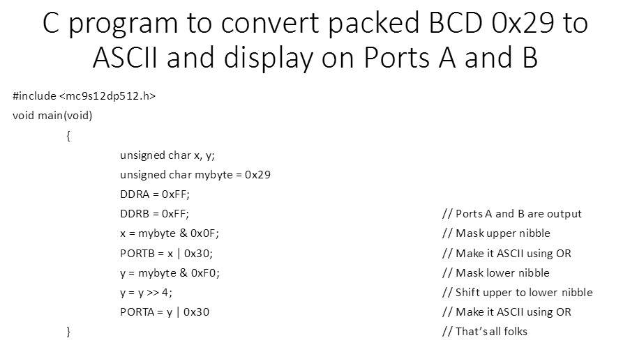
1、Packed BCD to ASCII Conversion

5-6 Signed Number Concepts and Arithmetic Operation
1、Represent -128 D
; Representation of -128 D
; 1000 0000 128 in unsigned binary
; 0111 1111 1’s compliment
; 0000 0001 Add 1 for 2’s compliment
;1000 0000  Result is 80 H and N = 1
; Note that 128 D unsigned = signed -128 D
2、Byte sized signed number ranges, recall the -128 to +127 range of conditional branches

16 Bit Signed Numbers

3、When is the overflow flag set?
•Either of the following conditions cause V = 1
1. There is a carry from Bit 6 to Bit 7 but no carry from Bit 7
2. There is a carry from Bit 7 but no carry from Bit 6 to Bit 7
•Note in either case we do not have a carry from both
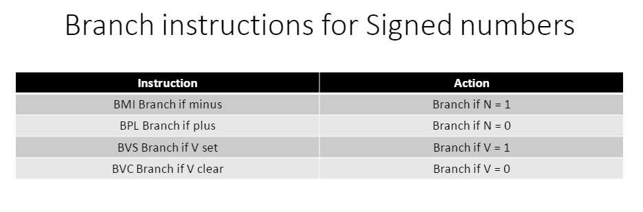
4、Branch instructions for Signed numbers
5、ASLA vs LSLA
- These two instructions do exactly the same thing
– There is really no need for ASL as far as signed numbers are concerned
6、Signed Number Comparison

7、Branch instructions for Signed Numbers

8、Multiplication of Signed Numbers

9、Signed Number Division

六、Chapter 6 Advanced Addressing Modes, Look up Table, Macros and Modules
6-1 Addressing Mode 比较
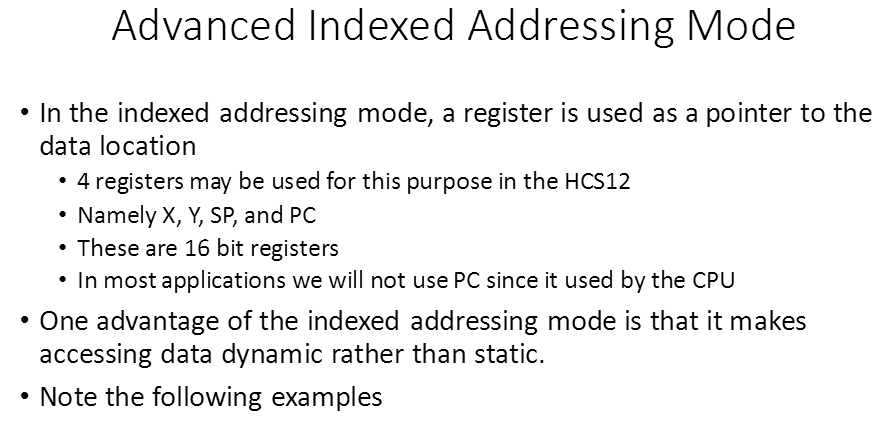
1、Advanced Indexed Addressing Mode
栗子:

Comments about previous example
•Using a loop is most efficient in the general case
•This is only possible because of the indexed addressing mode •Looping is not possible in extended addressing mode
•This is the main difference between extended and indexed modes
•Think about the case where we might want to send a string
•This would much more efficient using indexed mode
•Note the next example
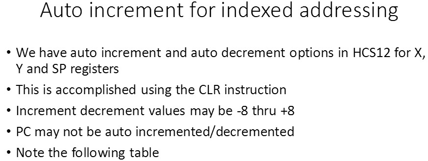
2、Auto increment for indexed addressing
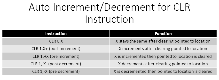
3、Auto Increment/Decrement for CLR Instruction
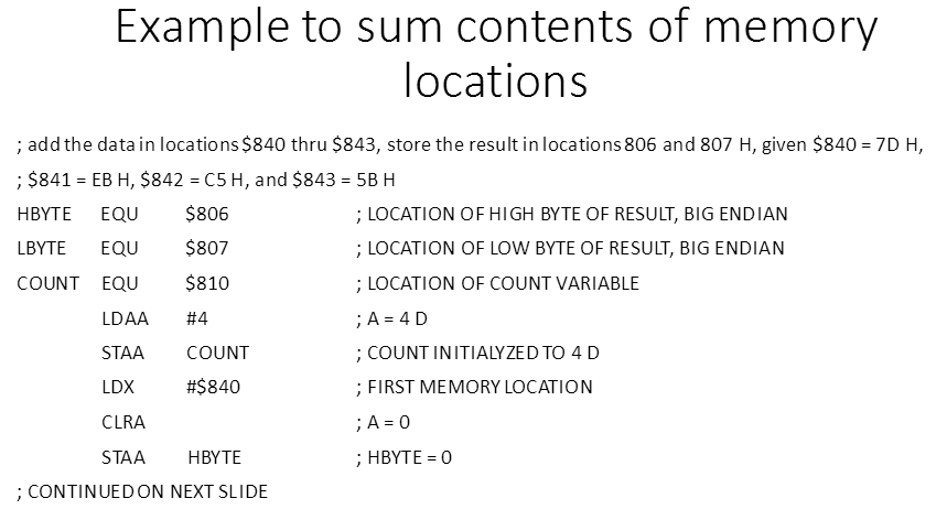
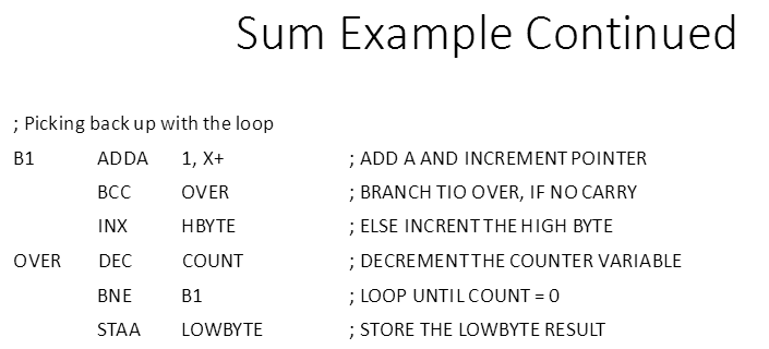
4、Example to sum contents of memory locations
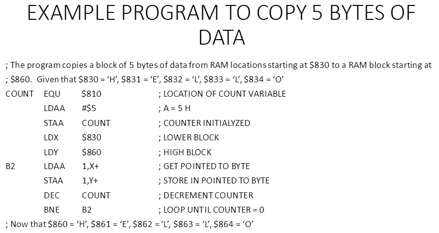
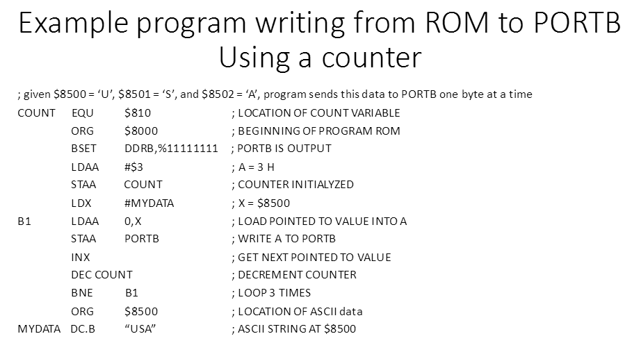
5、EXAMPLE PROGRAM TO COPY 5 BYTES OF DATA
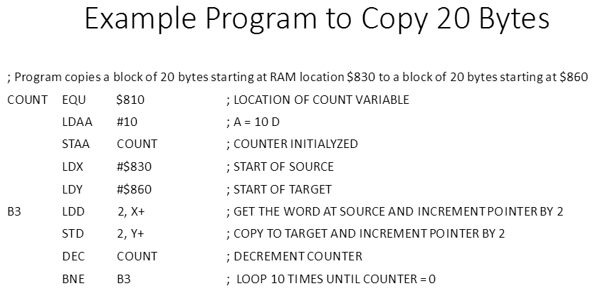
6、Example Program to Copy 20 Bytes
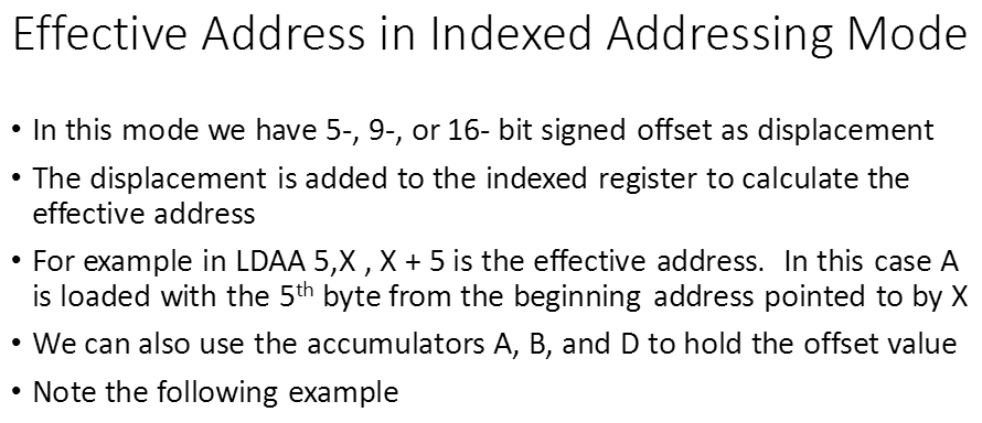
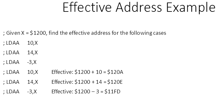
7、Effective Address in Indexed Addressing Mode
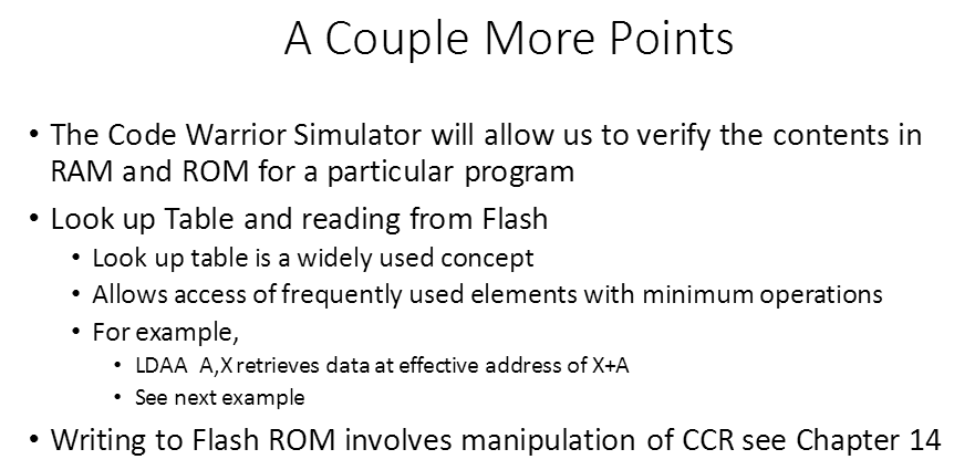
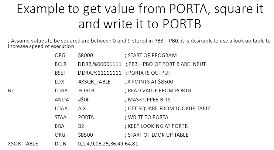
6-2 Accessing Look Up Table in Flash
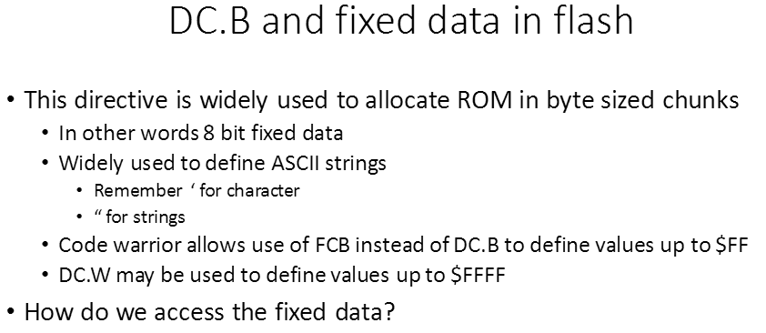
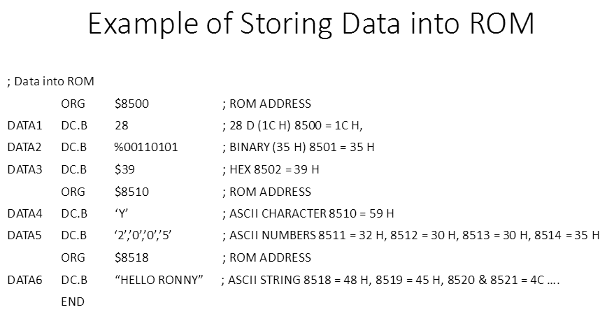
1、DC.B and fixed data in flash
2、栗子
这样都不需要count了,直接用NULL哨兵控制
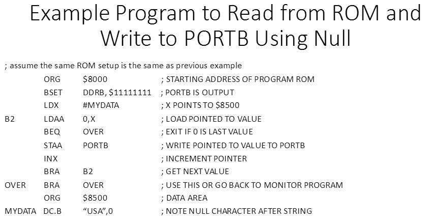
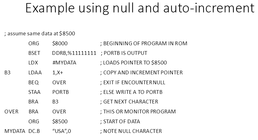
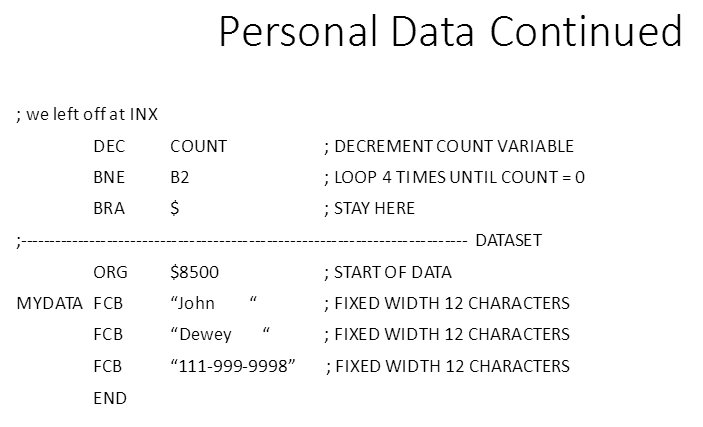
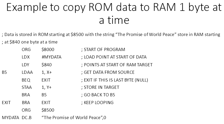
3、Look up table
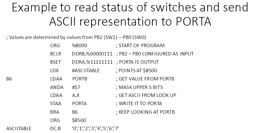
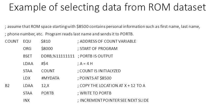
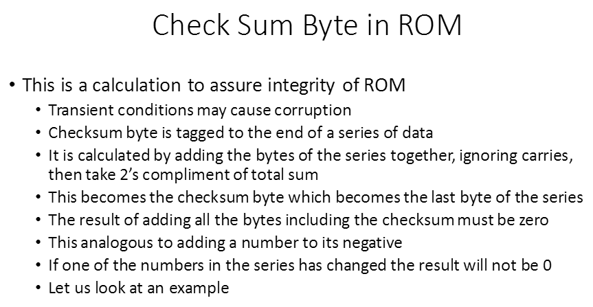
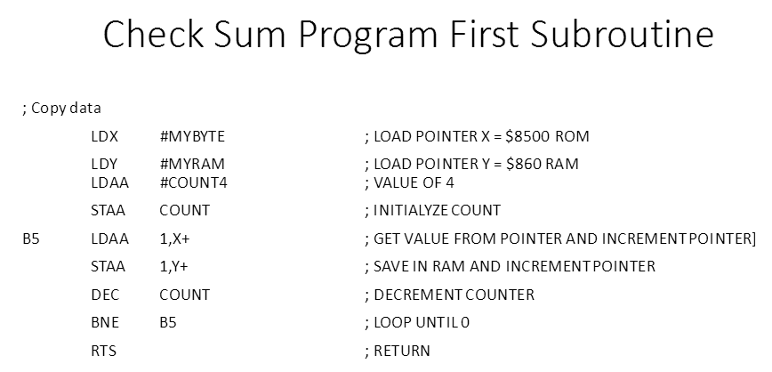
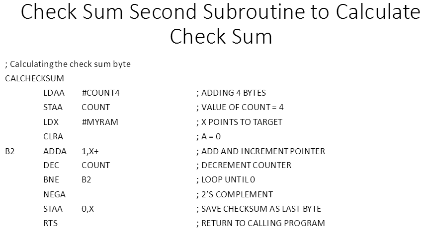
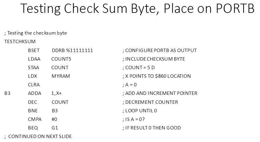
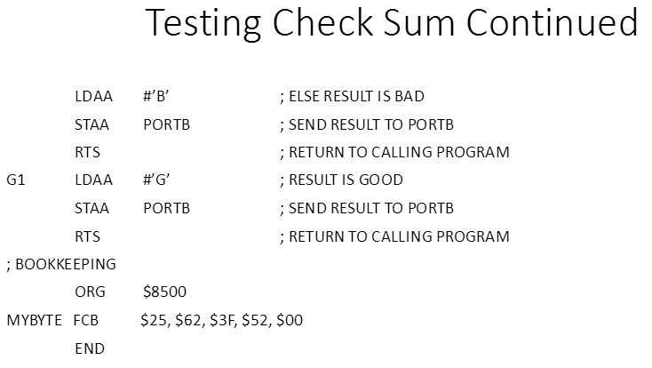
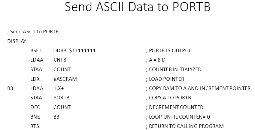
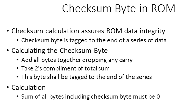
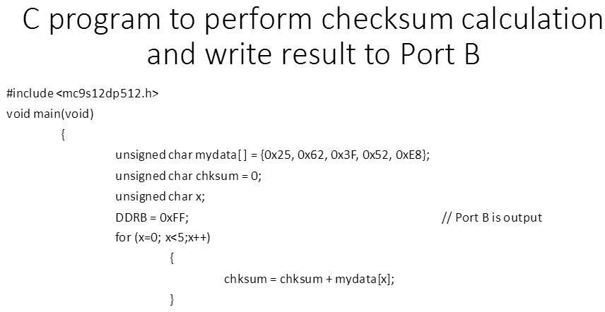
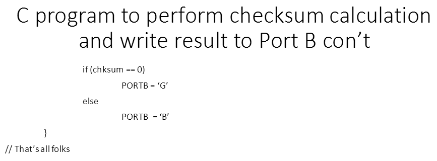
6-3 Checksum and ASCII Subroutines(栗子章节)
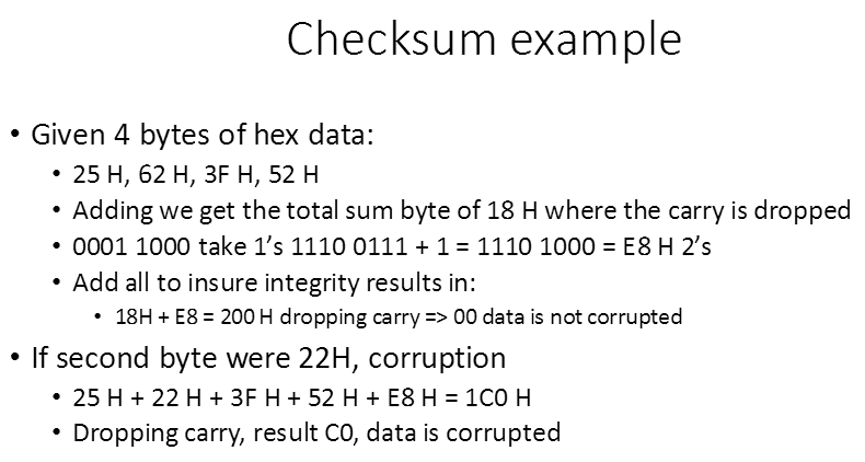
1、Check Sum Byte in ROM
25 H, 62 H, 3F H, 52 H 的和为 118H

2、BCD to ASCII Conversion

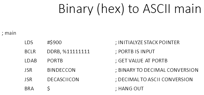
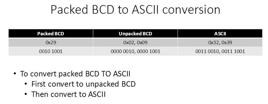
3、Binary (hex) to ASCII
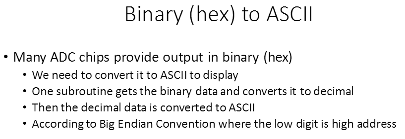
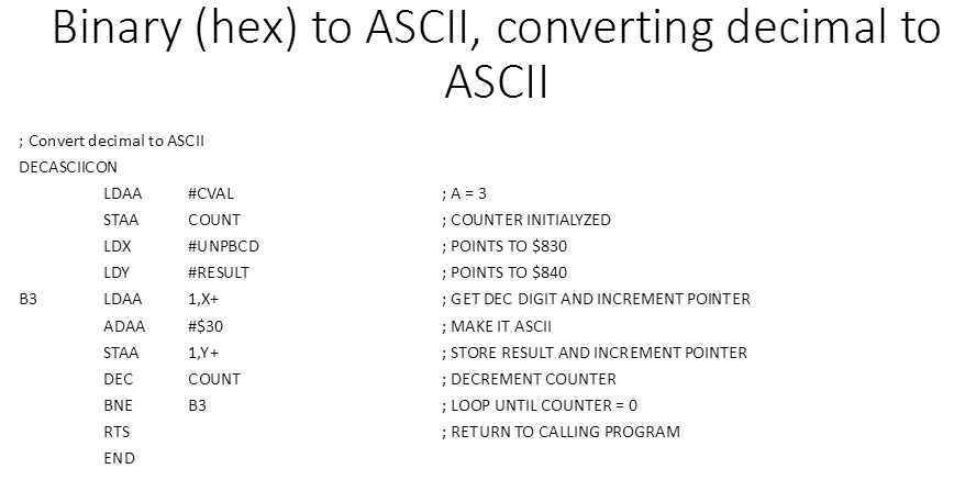
bcd码通常是指8421码就是将十进制的数以8421的形式展开成二进制,大家知道十进制是0~9十个数组成,这十个数每个数都有自己的8421码
bcd码是四位二进制码, 也就是将十进制的数字转化为二进制, 但是和普通的转化有一点不同, 每一个十进制的数字0-9都对应着一个四位的二进制码,对应关系如下: 十进制0 对应 二进制0000 ;十进制1 对应二进制0001 ……. 9 1001 接下来的10就有两个上述的码来表示 10 表示为00010000 也就是BCD码是遇见1001就产生进位,不象普通的二进制码,到1111才产生进位10000
压缩BCD码与非压缩BCD码的区别—— 压缩BCD码的每一位用4位二进制表示,一个字节表示两位十进制数。例如10010110B表示十进制数96D;非压缩BCD码用1个字节表示一位十进制数,高四位总是0000,低4位的0000~1001表示0~9.例如00001000B表示十进制数8.
百度百科http://baike.baidu.com/view/45179.htm?fr=ala0_1_1
BCD码代表数字0~9,ASCII码中也有代表数字0~9的码元,可以查看ASCII表,’0’=48,’1’=49,依次类推。
先把压缩BCD拆开变成非压缩BCD,然后加48就是ASCII中的0~9了!
所以反而类似于“所见即所得”了:
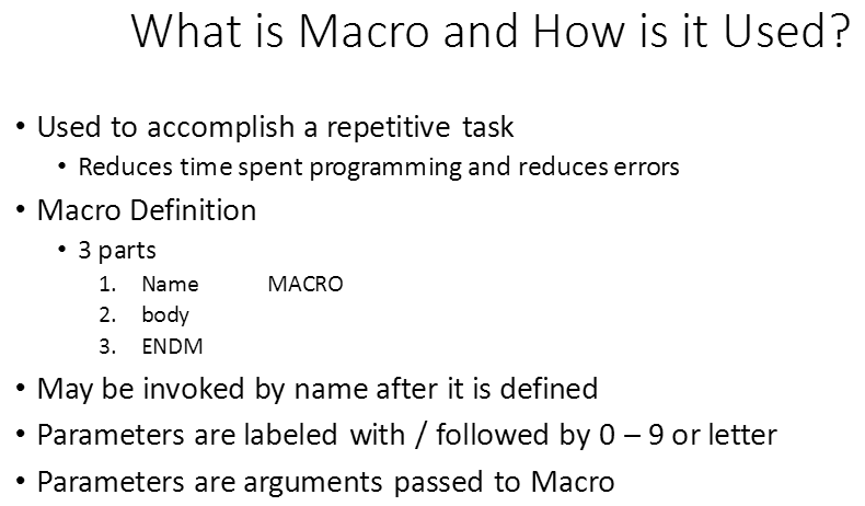
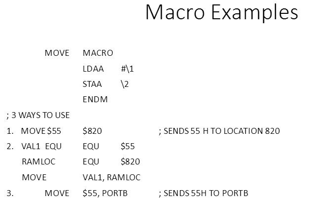
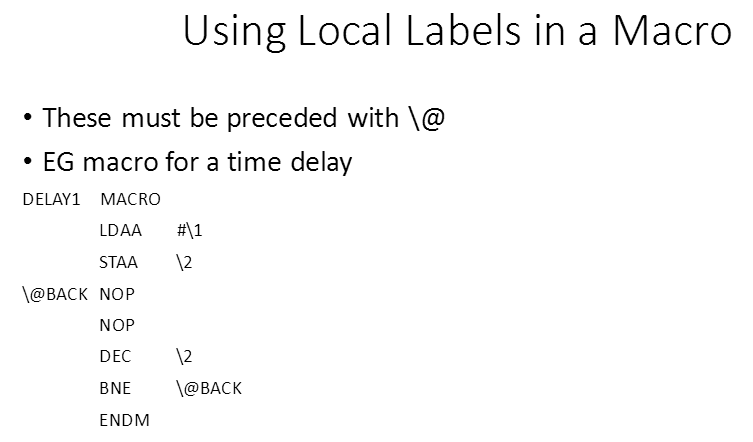
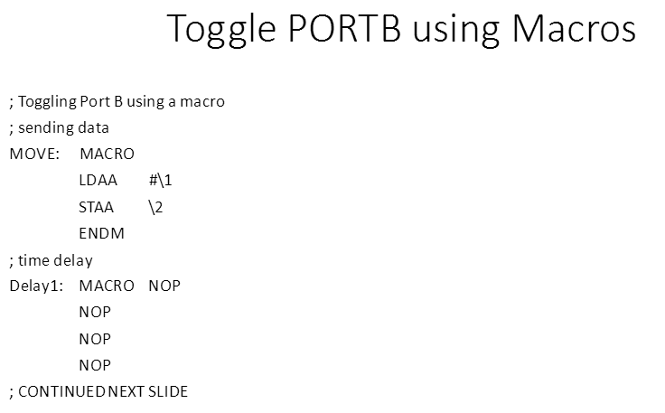
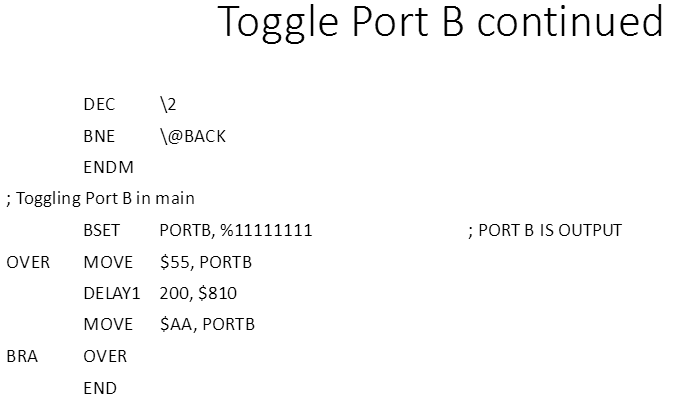
6-4 MACROS and MODULES
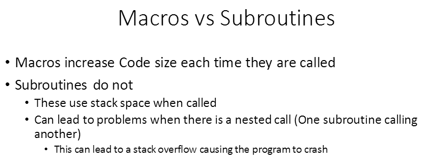
1、What is Macro and How is it Used?
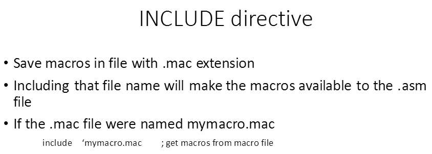
2、INCLUDE directive
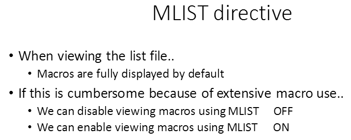
3、MLIST directive
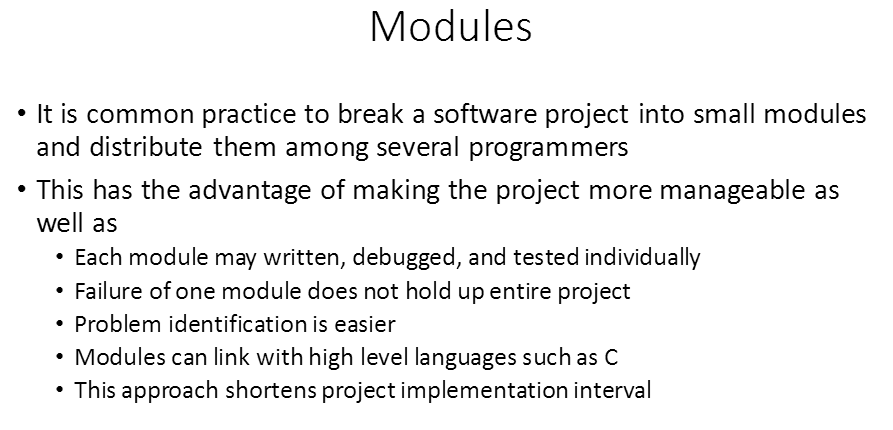
4、Modules

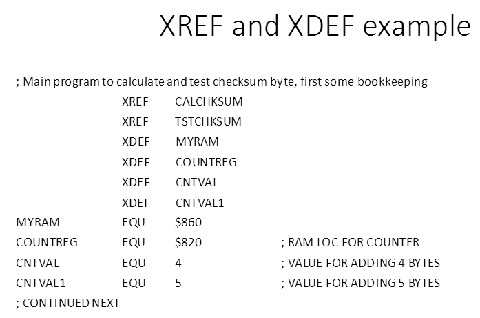
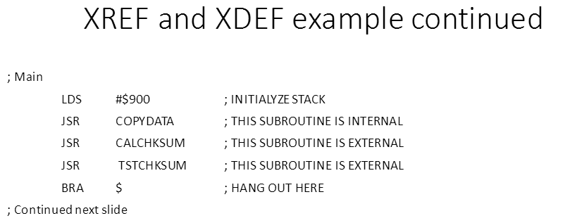
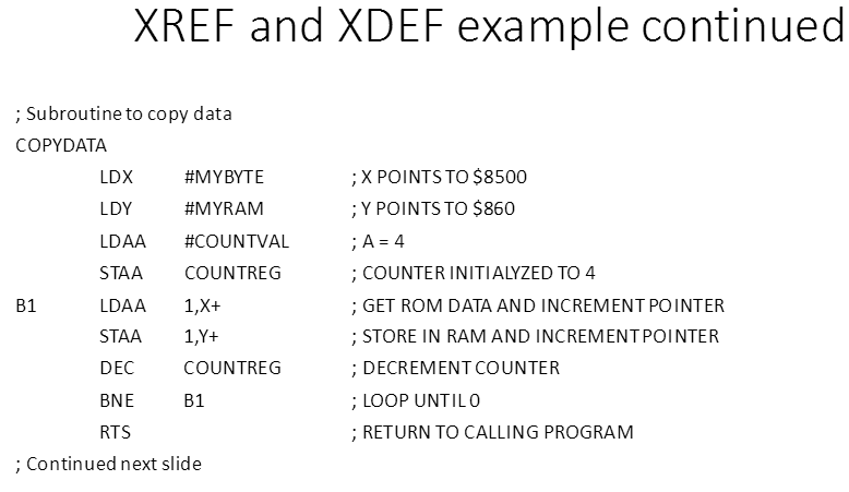
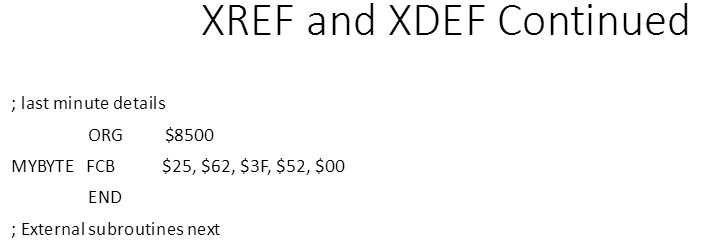
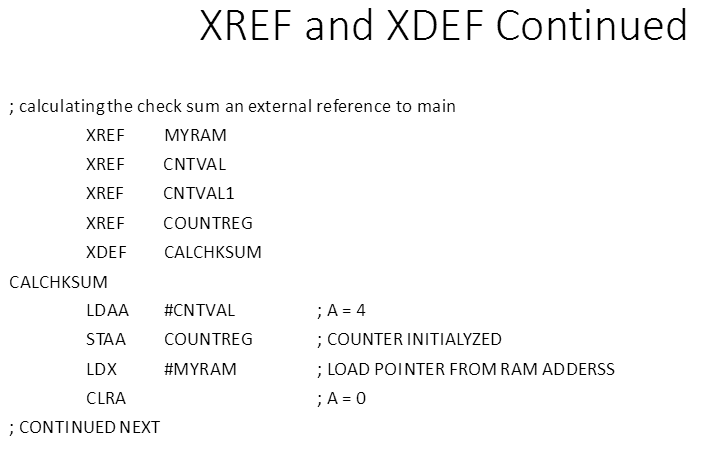
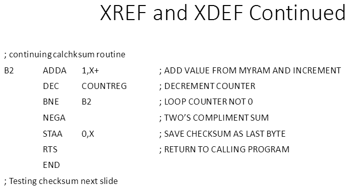
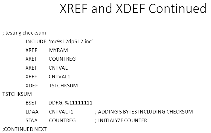
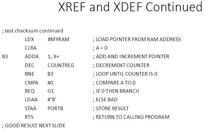
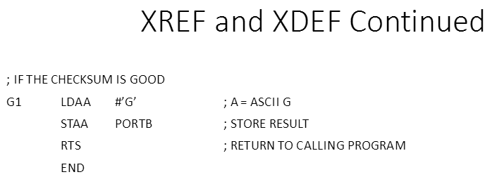
5、XREF and XDEF example
Linking modules in Code Warrior
•This is accomplished by copying the related .asm files into the source folder in code warrior.
七、Chapter 7 HCS12 Programming in C
7-1
1、关于 unsigned char
•Character data type is most natural type for many applications.
•Unsigned character type is one of the most used in HCS12 programming
•C compilers default to character type unless keyword “unsigned” is used
•Programmers should use unsigned character over other data types whenever possible
2、Signed Characters
•8 bit data type representing signed 7 bit numbers
•MSB contains sign, if 0 then positive, if 1 then negative
•Values -128 to +127 may be represented
•Must be used when we are dealing with any data that may take on a value in the above range
•This the default character data type
3、Unsigned integer
•16 bit data type •Range is 0000 – FFFF H
•Typically used to define 16 bit variables such as data addresses •Also useful for counter value > 256
•Use it sparingly
•Use the unsigned variant if negative numbers not expected
•C compiler defaults to signed integer
4、Time Delay
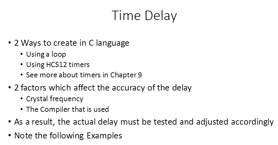
250 ms delay assuming 2 MHz clock
void MSDelay(unsigned int itime)
{unsigned int i; unsigned int j; for (i=0; i<itime; i++) for (j=0; j<331; j++);
}
// concludes example
7-2 Bitwise Logic Operations in C
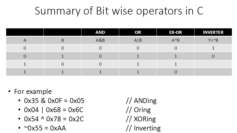
1、Summary of Bit wise operators in C
7-3 Data conversion programs in C
1、Packed BCD to ASCII conversion
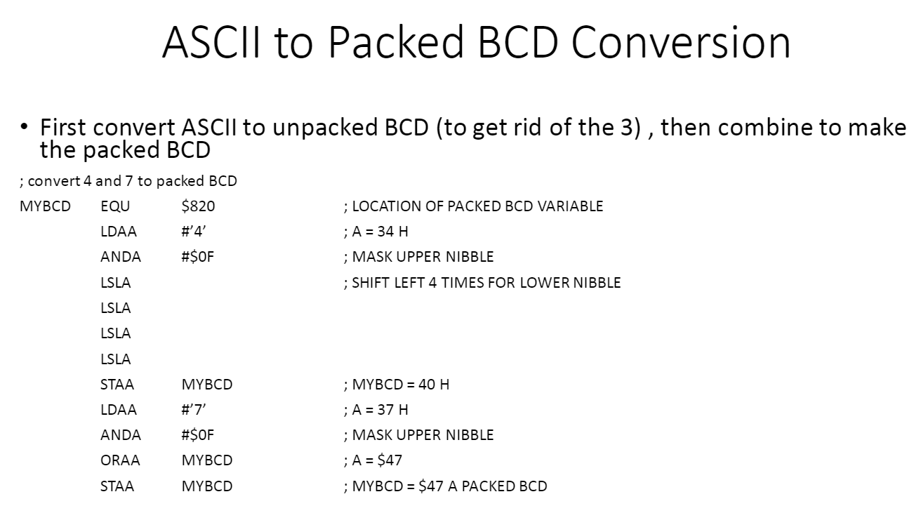
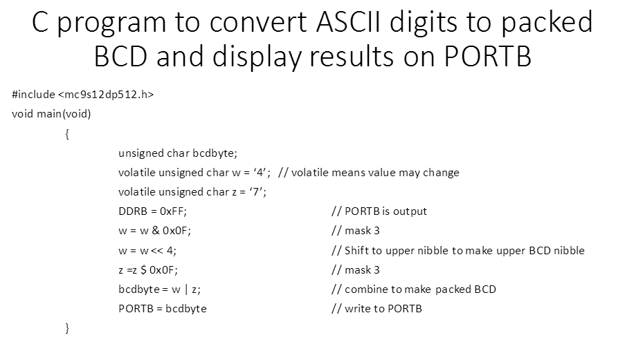
2、ASCII to Packed BCD conversion
3、Checksum Byte in ROM
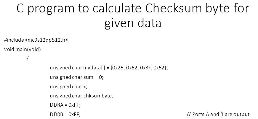
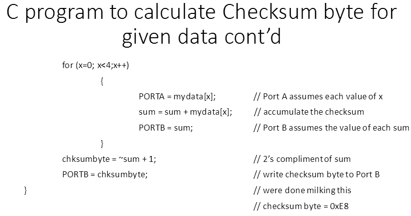
perform checksum calculation
4、C program for Binary (Hex FD) to Decimal Conversion
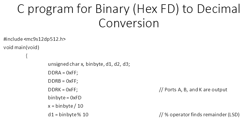
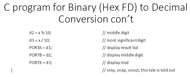
7-4 I/O bit manipulation and data serialization in C
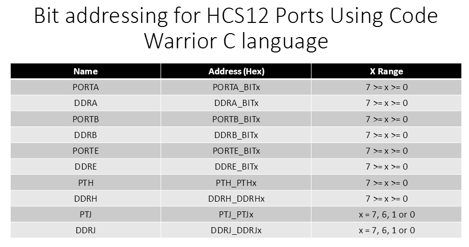
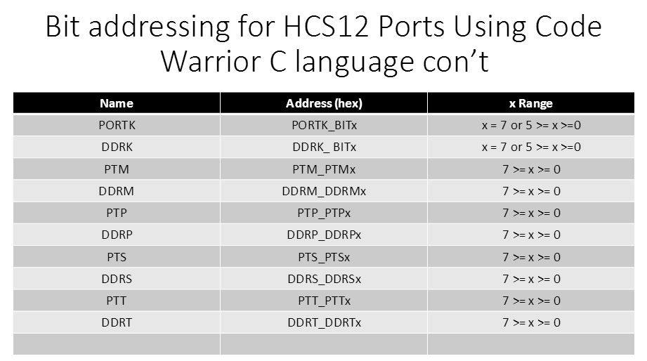
1、Bit addressing for HCS12 Ports Using Code Warrior C language
7-5 Program ROM allocation in C
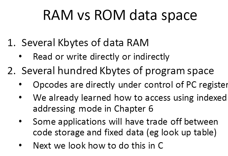
1、RAM vs ROM data space
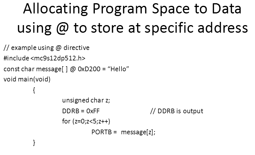
2、Allocating Program Space to Data using @ to store at specific address
附录:
常用重要标签汇总
1、Load and Store Instructions
2、CCR register
3、分支语句(1)CCR基本跳转
4、DC.B
5、Stack Instructions & Data Transfer Instructions
6、MC9S12Dx256 内存图
7、Auto Increment/Decrement for CLR Instruction
8、分支语句(2)LOOP基本跳转
9、分支语句(3)Long Conditional Branches
10、HCS12 Call Instruction Summary
11、Ports in the MC9S12D Family
12、Some Widely Used Arithmetic Instructions
13、Unsigned Multiplication and Division Summary
课件地址:https://github.com/billhhh/hcs12_dragon12_asm/tree/master/PPT
示例代码地址:
http://www.microdigitaled.com/HCS12/Hardware/Dragon12/CodeWarrior_asm/
这篇关于hcs12 microcontroller 笔记的文章就介绍到这儿,希望我们推荐的文章对编程师们有所帮助!