本文主要是介绍USB - USB在消费领域的应用,希望对大家解决编程问题提供一定的参考价值,需要的开发者们随着小编来一起学习吧!
Switching in USB Consumer Applications
通用串行总线(USB)已成为满足终端设备之间日益增长的快速数据传输需求的主流接口--例如,在个人电脑和便携式设备(如手机、数码相机和个人媒体播放器)之间下载和上传数据。
| The universal serial bus (USB) has become a dominant interface to fulfill the ever increasing needs for rapid data transfer between end devices—for example, downloading and uploading data between PCs and portable devices such as cell phones, digital cameras, and personal media players. |
CMOS 开关可用于 USB 系统中数据线的连接和布线。通过选择合适的开关,设计人员可以增强现有设计而不是开发新设计,从而大大缩短设计周期。在本文中,我们将介绍 USB,然后探讨开关在提高便携式媒体播放器、手机和无线笔式驱动器等应用的性能方面所起的关键作用。我们还展示了开关的关键参数对整个系统设计的影响,并讨论了基本的设计挑战,如满足带宽要求与最大限度减少信号反射之间的权衡。此外,我们还建议如何通过精心的电路板布局最大限度地扩大眼图的开口。
| CMOS switches can be used for connecting and routing data lines in USB systems. By selecting suitable switches, designers can significantly shorten design cycles by enhancing existing designs rather than developing new ones. In this article, we describe the USB, then go on to explore the crucial role of switches in improving performance in applications such as portable media players, cell phones, and wireless pen drives. We also show how key parameters of the switches affect the overall system design and discuss basic design challenges, such as the trade-offs between meeting bandwidth requirements and minimizing signal reflections. Additionally, we suggest how to maximize the opening in eye diagrams by careful board layout. |
What Is USB and Why Has It Become So Popular?
USB 已成为全球最流行的 PC 与外设通信标准。键盘、打印机、数据存储设备和手机等众多外围设备都可以通过 USB 标准连接到个人电脑。以前使用串行端口和并行端口的设备正在向 USB 迁移,同时硬盘驱动器和数码相机等设备的设计者通常会选择 USB 而不是其他标准,如火线或串行端口通信。与手机、MP3 播放器和游戏机的连接也是最近的一项发展。
| USB has become the most popular standard for PC-to-peripheral communication in the world. Keyboards, printers, data-storage devices, and mobile phones are among the many peripherals that can be connected to a PC, employing the USB standard. Devices that previously used serial ports and parallel ports are migrating to USB, while designers of devices such as hard drives and digital cameras are often choosing USB over other standards, such as FireWire or serial-port communication. Connectivity to mobile phones, MP3 players, and game consoles is another recent development. |
USB 的主要魅力在于即插即用。将设备插入个人电脑,由个人电脑识别;然后,在首次安装适当的软件后,设备将始终被主机识别--这是一种用户友好的握手方式。
| USB’s main attraction is the ability to plug and play. The device is plugged into the PC, recognized by the PC; then, after the first installation of appropriate software, the device will always be recognized by the host PC—a user-friendly handshake. |
USB 实施者论坛公司是一个由计算机和电子行业领先公司赞助的行业标准制定机构,负责制定 USB 标准。设备设计可以获得 USB 认证并在产品上使用 USB 标志,但必须通过非常严格的软件和硬件测试。这确保了所有通过 USB 认证的设备,无论是个人电脑还是外围设备,都能从软件和硬件两个角度正确地进行互联。该标准确保所有经过认证的软件程序、连接器、电缆、信号驱动程序和接收器都符合标准,从而保证了互联性(图 1a)。
| The USB Implementers Forum, Inc., an industry-standard-generating body sponsored by leading companies from the computer and electronics industry, lays down the standards for USB. Device designs can receive USB certification—and use the USB symbol on a product, but only after passing very strict software and hardware tests. This ensures that all USB-certified devices, whether PC or peripheral, will function correctly when interconnected, from the standpoints of both software and hardware. The standard ensures that all certified software routines, connectors, cables, signal drivers, and receivers comply, ensuring interconnnectability (Figure 1a). |
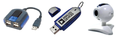
Figure 1a. USB devices: a port expander, a pen drive, and a webcam.
USB 基于串行主从架构。一般来说,PC 是主设备,称为主机(图 1b);它控制各项作业。被称为外设的从设备告诉主机其带宽需求,然后开始数据交换。正常 USB 事件的完整序列包括以下步骤:
1. 外设插入主机(启动 USB 事件)
2. 握手(识别外设、分配带宽)
3. 批量数据传输(如传输至打印机),或外设轮询(鼠标)
4. 主机禁用外设
5. 外设断开连接
| USB is based on a serial master-slave architecture. In general, the PC is the master, known as the host (Figure 1b); it controls the transaction. The slave, known as the peripheral, tells the host its bandwidth requirement, and then a data transaction is initiated. A complete sequence of normal USB events includes these steps: 1. Peripheral plugged into host (initiating USB event) 2. Handshaking (peripheral identified, bandwidth allocated) 3. Bulk data transfer (e.g., to printer), or peripheral polled (mouse) 4. Peripheral disabled by host 5. Peripheral disconnected |

Figure 1b. Typical host- and peripheral USB devices.
USB 系统中使用的硬件通过双线(加地线)差分双向系统传输数据。数据线 D+ 和 D- 传输数据,如图 2 所示。数据只能单向传输,因此在一种情况下,主机传输数据的同时外设接收数据,然后外设传输数据的同时主机接收数据。USB 标准还包括一条 5 V 电源线。一般用于为下游设备供电,使 USB 笔式驱动器、网络摄像头和键盘等低功耗设备不再需要电池。
| The hardware used in a USB system transmits data using a 2-wire (plus ground) differential bidirectional system. The data lines, D+ and D–, transmit the data as shown in Figure 2. Data can only be transmitted in one direction, so in one instance the host transmits while the peripheral receives, and then the peripheral transmits while the host receives. The USB standard also includes a 5-V power line. Generally used to power downstream devices, it obviates the need for batteries in low-power devices such as USB pen drives, webcams, and keyboards. |
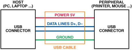
Figure 2. USB interconnections.
How Do USB 1.1 and USB 2.0 Compare?
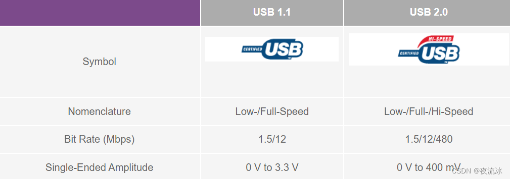
USB 标准规定了三种数据传输速率: 低速(1.5 Mbps)、全速(12 Mbps)和高速(480 Mbps)。USB 1.1 设备的信号电平为 ±3.3-V,可以低速和全速运行。USB 2.0 设备的信号电平为 ±400-mV,可以低速、全速和高速运行。
| The USB standard specifies three data rates: Low-Speed (1.5 Mbps), Full-Speed (12 Mbps), and Hi-Speed (480 Mbps). USB 1.1 devices have ±3.3-V signal levels and can operate at low- and full speeds. USB 2.0 devices have ±400-mV signal levels and can operate at low-, full-, and high speeds. |
Table I. Comparison of USB 1.1 and USB 2.0
What Is USB On-The-Go (USB OTG)?
许多消费产品,如作为 USB 外围设备连接到电脑的手机和数码相机,也可以连接到其他 USB 设备。在这种情况下,个人电脑无法充当主机,因此需要由其中一个外设来承担责任。USB OTG 定义了一种双重角色的设备,它既可以充当主机,也可以充当外设,而且可以使用相同的连接器连接电脑和其他便携设备。
| Many consumer products—such as cell phones and digital cameras, that connect to the PC as a USB peripheral—can also be connected to other USB devices. Since, in these circumstances, the PC cannot be the host, one of the peripherals needs to take on the responsibility. USB OTG defines a dual-role device, which can act as either a host or a peripheral—and can use the same connector for both PCs and other portable devices. |
通过实现数字设备之间的基本功能,USB OTG 使这些 PC 外围设备的功能更强大,因此对消费者和企业用户来说更有价值。USB OTG 设备当然可以连接个人电脑,因为它们符合 USB 2.0 规范。此外,它们还具有有限的主机功能,可以连接到一系列目标明确的其他 USB 外围设备。当两个双重角色设备通过电缆连接在一起时,电缆会设置默认主机和默认外设。如果应用要求转换角色,主机协商协议(HNP)会提供一个握手来执行该功能,这种转换对用户来说是完全不可见的。
| By enabling basic functions between digital devices, USB OTG makes these PC peripherals more capable, hence more valuable to consumers and corporate users. USB OTG devices will, of course, connect to PCs, as they comply with the USB 2.0 specification. In addition, they will have limited host capability to allow them to connect to a targeted set of other USB peripherals. When two dual-role devices get connected together via a cable, the cable sets a default host and default peripheral. If the application requires that the roles be reversed, the Host Negotiation Protocol (HNP) provides a handshake to perform that function, a reversal completely invisible to the user. |
What Are the Switch Requirements for USB 1.1/USB 2.0?
USB 数据线 D+ 和 D- 可以通过内部 CMOS 开关连接和路由。在图 3 的示例中,每个数据线串联了一个开关。使用多路复用器还可提供额外的开关容量。低速、全速和高速 USB 使用 45 欧姆系统;驱动器的源阻抗为 45 欧姆,接收器对地的终端阻抗为 45 欧姆。所有 USB 电缆和轨道的单端阻抗都应为 45 欧姆,以保持信号完整性。稍后我们将讨论传输线阻抗和电路板布局。
| The USB data lines, D+ and D–, can be connected and routed by internal CMOS switches. In the example of Figure 3, a switch is connected in series with each data line. Additional switch capacity is available by using multiplexers. Low-, Full-, and Hi-Speed USB use a 45-ohm system; the driver has a source impedance of 45 ohms, and the receiver has a termination of 45 ohms to ground. All USB cables and tracks should have a single-ended impedance of 45 ohms to preserve signal integrity. We will discuss transmission-line impedance and board layout later. |
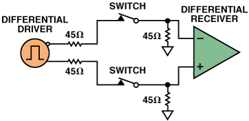
Figure 3. USB 45-ohm system.
USB 标准要求进行严格的测试,以确保信号处理符合其要求。其中一项关键测试是 "眼图"。这是一种直观的视觉测试,可以看出信号的质量。眼图是通过探测随机变化的数字信号,绘制其与一个或多个周期扫描的对比图,并将示波器设置为长时间持续扫描而生成的。其结果是,所有可能的比特排列都会叠加在一个视图上,显示出在振幅、相位、上升和下降时间上与理想 "眼图 "模式的偏差范围。因此,任何可能导致问题的比特模式都可以在图中看到。
| USB standards call for stringent tests to ensure that signals are handled in conformance with their requirements. One of the key tests is an “eye” diagram. This is an intuitive visual test, which can tell a lot about the signal’s quality. An eye diagram is generated by probing a randomly varying digital signal, plotting it vs. sweeps of one or more cycles, and setting the scope for long persistence. The result is that all possible bit permutations are overlaid on a single view, showing the range of deviations from an ideal “eye” pattern in amplitude, phase, and rise- and fall times. Hence any bit patterns that could cause problems may be seen on the plot. |
图 4 摘自 USB-IF 规范,显示了用于建立眼图的设置。USB-IF 分发的 "SQiDD"(信号质量下降/掉电)测试板充当主机;鼠标(被测设备)插入该测试板。探测信号 D+ 和 D-,然后将其叠加到示波器上,生成眼图。然后将眼图与所需形状的眼图进行比较,以便查看信号质量是否符合 USB 标准。
| Figure 4, taken from the USB-IF spec, shows the setup used to establish the eye diagram. The “SQiDD” (signal quality drop/droop) test board, which the USB-IF distributes, functions as a host; and the mouse (the device under test) is plugged into this board. The signals D+ and D– are probed, and then overlaid on the scope, generating the eye diagram. The eye opening is then compared with a mask of the required shape to allow the viewer to see if the signal quality complies with the USB standard. |

Figure 4. USB IF recommended eye-test setup.
在测试 CMOS 开关在 USB 产品中的适用性时,不能将其本身作为 USB 设备进行测试,因为它们是在设备内部的信号路径中使用的。因此,可以使用数据发生器来产生所需的信号,该信号通过开关后在示波器上终止。示波器使用外部时钟触发,外部时钟与随机数字信号同步。这将产生 CMOS 开关的眼图。
| In testing the suitability of CMOS switches for use in USB products, they cannot be tested by themselves as USB devices, since they are used within the device in the signal path. Therefore, a data generator could be used to generate the required signal, and this signal, passing through the switch, is terminated at the scope. The scope is triggered using an external clock, which is synchronized with the random digital signal. This will result in an eye diagram of the CMOS switch. |
例如,图 5 所示的一组典型眼图是在 USB 高速数据传输速率(480 Mbps)和信号电平(0 至 400 mV)条件下生成的。它们比较了通过相同信号的 ADG774A(带宽大于 500 MHz)和 ADG736(带宽 200 MHz)CMOS 开关的性能。图中包括一个 USB-IF 掩码(红色六边形)。根据 USB 规范,如果信号越过掩码的边界,器件的信号完整性就会失败。
| For example, a set of typical eye diagrams is shown in Figure 5, generated at USB Hi-Speed data rates (480 Mbps) and signal levels (0 to 400 mV). They compare the performance of ADG774A (bandwidth >500 MHz) and ADG736 (200-MHz bandwidth) CMOS switches, passing the same signals. Included in the plot is a USB-IF mask (red hexagon). According to the USB spec, if the signal crosses the boundaries of the mask, the device fails on signal integrity. |
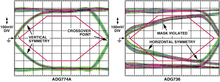
Figure 5. Comparison of the ADG774A and ADG736 at USB Hi-Speed.
从图中可以看出,ADG774A 符合掩码要求,即使在如此高的数据速率下也几乎没有波纹。然而,ADG736 由于电容较大、带宽较低,边缘速度较慢,从而导致信号在左侧穿过掩码--这显然违反了规定,使其不符合用于传递高速 USB 信号的条件。其他值得注意的信息是 ADG736 眼缺乏水平对称性,而 ADG774A 即使在如此高的数据速率下也相当对称。不过,两个开关的垂直对称性都很好,这表明两个器件上的两个通道匹配良好。在为 USB 应用选择开关时,通道匹配是一个非常重要的问题。在差分系统中,D- 信号必须与 D+ 信号完全相反。D+ 和 D- 线路之间的电缆长度、电容和电阻不匹配会造成严重的偏斜,表现为垂直不对称。信号交叉点(分频点)应以接地为中心。抖动对 USB 鉴定也至关重要。边缘越厚,抖动越严重,而这些 CMOS 开关却没有问题。实际上,移除开关后也能看到抖动,这表明系统中存在抖动。
| The illustration shows that the ADG774A complies with the mask, displaying little ripple, even at these high data rates. The ADG736, however, with its higher capacitance and lower bandwidth, has slowed down the edges, thereby causing the signal to cross the mask on the left side—a clear violation, which disqualifies it from being used to pass Hi-Speed USB signals. Other noteworthy information is the lack of horizontal symmetry in the ADG736 eye, whereas the ADG774A is quite symmetrical, even at this high data rate. Both switches exhibit good symmetry vertically, however, which would indicate good matching of the two channels on both devices. Channel matching is a big concern when selecting a switch for USB applications. In a differential system, the D– signal must be the exact inverse of the D+ signal. Mismatches in cable length, capacitance, and resistance between the D+ and D– lines can cause serious skew in the eye, manifested as vertical asymmetry. The point where the signals cross (the crossover point) should be centered on ground. Jitter is also critical to USB qualification. The thicker the edges, the worse the jitter—not a problem with these CMOS switches. Actually, the jitter seen was also visible with the switch removed, suggesting that the jitter exists in the system. |
图 6 是 ADG787 使用 USB 全速信号(0 V 至 3 V,12 Mbps)的典型曲线图,其设置与上述曲线图类似。所示掩码取自 USB-IF 的 USB 全速规格。所用信号的上升和下降时间为 6 纳秒。可以看出,信号没有出现上述故障。没有违反眼图遮罩要求,抖动良好,交叉和对称性良好,波纹很小。这些图显示了眼图的价值,因为我们可以一目了然地得出结论:ADG787 可以轻松通过全速 USB 信号。
| Figure 6 is a typical plot for an ADG787, using a USB Full-Speed signal (0 V to 3 V, 12 Mbps) in a setup similar to the one used for the above plots. The mask shown is taken from the USB-IF spec for USB Full Speed. The signal used had a rise- and fall time of six nanoseconds. As can be seen, the signal is free from the faults discussed above. No mask violation, good jitter, good crossover and symmetry, and little rippling can be observed. These plots demonstrate the value of an eye diagram, in that at a glance we can conclude that this ADG787 can easily pass a Full-Speed USB signal. |

Figure 6. Eye diagram of the ADG787 at USB Full Speed.
How to Choose a CMOS Switch for USB Applications
现在我们来说明开关的具体要求及其对信号的影响。本节将讨论开关规格与整个系统信号完整性之间的相互关系。
两种标准对开关的要求都是导通电阻越低越好,同时还要有低电容。两个开关的特性需要尽可能精确地匹配,以保持数据线的对称性。
| We now illustrate the specific requirements of a switch and how they affect the signal. This section will consider the correlation between switch specifications and overall system signal integrity. Switch requirements for both standards would call for as low an on resistance as possible, combined with low capacitance. The characteristics of the two switches need to be matched as accurately as possible to keep the data-line symmetry. |
On Resistance
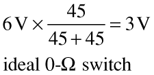
在 45 欧姆系统中,导通电阻不宜大于 5 欧姆,因为 5 欧姆的导通电阻会增加信号源阻抗,使其达到 50 欧姆。为了让接收器接收 3 V 信号,45 欧姆信号源传输 6 V 信号,理想情况下,45 欧姆信号源和终端阻抗形成的分压器将信号减半。如图 7 所示,开关与驱动器串联为一个电阻。在串联 5 欧姆的情况下,接收器看到的是 50 欧姆的信号源和 45 欧姆的接地电阻。
| In a 45-ohm system, an on resistance of greater than 5 ohms is undesirable, as a 5-ohm on resistance will add to the source impedance, making it 50 ohms. In order for the receiver to receive a 3-V signal, the 45-ohm source transmits a 6-V signal, which is ideally halved by the divider formed by the 45-ohm source and the termination impedance. This is illustrated in Figure 7, which shows the switch as a resistance in series with the driver. With 5 ohms in series, the receiver sees a 50-ohm source and 45 ohms to ground. |

Figure 7. Model of the switch as a resistor
这些公式比较了理想开关和串联电阻为 5 欧姆的开关的性能。开关会带来很大的损耗(>5%)。因此,低Ron是至关重要的。
| The equations compare performance of an ideal switch with one having 5 ohms of series resistance. A significant loss (>5%) is introduced by the switch. Therefore low Ron is critical. |

CMOS 开关的源极至漏极电阻随电源电压和偏置电压而变化,如 ADG787 开关的 Ron 图所示。随着源极电压的变化,从源极到漏极测量到的电阻也随之变化。
| The source-to-drain resistance of a CMOS switch varies with both the supply voltage and the bias voltage, as illustrated in the Ron plot for an ADG787 switch. As the voltage on the source is varied, the resistance measured from source to drain changes. |
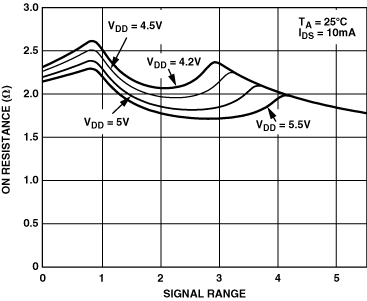
Figure 8. On-resistance variation over input source voltage of the ADG787.
如果开关的电阻随偏置电压、温度或电源的变化而变化,接收器看到的振幅也会随之变化,如变化的Ron(即Ron + Δ Ron)所示。
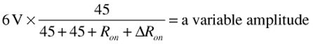
| If the resistance of the switch varies, with either bias voltage, temperature, or supply, the amplitude seen by the receiver will also vary, as can be seen for a varying Ron (i.e., Ron + Δ Ron). |
Ron平坦度对于确保开关的上升和下降时间尽可能接近也至关重要。如果Ron随偏置变化很大,上升沿和下降沿在其转换的不同阶段就会出现不同的阻抗。这种差异在眼图中将表现为不良的交叉。
| Ron flatness is also vital to ensuring that the rise- and fall times of the switch are as close as possible. If Ron varied significantly with bias, the rising and falling edges would see different impedances at different stages in their transition. Differences here would be seen as poor crossover in the eye diagram. |
因此,在设计用于 USB 产品的开关时,Ron 随电源电压、温度和偏置的变化是一个重要的考虑因素。在眼图上,Ron 随电源容差和温度的变化表现为抖动。通常情况下,Ron 越低,平坦度和失真越低,对比图 9(ADG836)和图 8 即可看出。ADG836 是在 0.35 微米几何尺寸上制造的双 SPDT 开关,其 Ron 值约为 0.5 欧姆,平坦度为 0.05 欧姆,而 ADG787 的 Ron 值为 2 欧姆,平坦度为 0.25 欧姆。保持低Ron是保持低Ron平坦度的关键。
| Therefore, Ron variability with supply voltage, temperature, and bias are big considerations when designing a switch for use in USB products. Variability of Ron over supply tolerances and temperature would be seen on the eye diagram as jitter. As a rule, lower Ron means lower flatness and distortion, as can be seen by comparing Figure 9 (ADG836) with Figure 8. The ADG836, which is a dual-SPDT switch fabricated on a 0.35-µm geometry, has Ron of about 0.5 ohms and 0.05-ohm flatness, compared with 2 ohms and 0.25-ohm flatness for the ADG787. Keeping Ron low is the key to keeping Ron flatness low. |
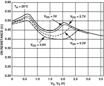
Figure 9. Ultralow on resistance of the ADG836 ensures excellent on resistance flatness.
在设计时,应尽可能紧密地匹配通道,以确保传递差分信号的两个开关通道的 Ron 和 ΔRon 相同。眼图可以显示出电阻匹配不佳。
| Channels should be matched as closely as possible when designing, to ensure Ron and ΔRon are the same for the two switch channels passing the differential signals. An eye diagram would indicate poor matching of on resistances. |
Capacitance 容值
CMOS 开关在导通状态下的电容随着开关尺寸的增大而增大。然而,由于低导通电阻是通过增大开关尺寸来实现的,因此Ron和电容之间存在直接的权衡。电容决定了开关的带宽,对于高速 USB 信号而言,电容变得更加重要,开关电容超过 10 pF 会显著降低信号质量。高电容会减慢边缘速度,导致眼睛越过遮罩范围。从图 5 的 ADG736 和 ADG774A USB 高速眼图对比中可以看出这一点。ADG736 的带宽为 200 MHz。ADG774A 的电容要小得多,带宽为 400 MHz。USB 全速要求 -3dB 开关带宽大于 6 MHz(12 Mbps),高速 USB 要求 240 MHz(480 Mbps)。布局工程师需要确保开关布局非常接近,以保持电容对称。
| Capacitance of CMOS switches in the on state increases with size of the switch. However, since low on resistance is achieved by increasing the size of the switch, there is a direct trade-off between Ron and capacitance. This capacitance, which dictates the bandwidth of the switch, becomes more critical for Hi-Speed USB signals, where switch capacitance greater than 10 pF can significantly degrade the signal. The high capacitance slows the edges down, causing the eye to cross the mask. This was seen in the comparison of the ADG736 and the ADG774A USB Hi-Speed eye diagram of Figure 5. The ADG736 has a bandwidth of 200 MHz. The ADG774A has a much lower capacitance with a bandwidth of 400 MHz. A –3dB switch bandwidth of greater than 6 MHz (12 Mbps) is required for USB Full Speed, with 240 MHz (480 Mbps) required for Hi-Speed USB. The layout engineer needs to ensure very close similarity of switch layouts to maintain symmetry capacitively. |
Propagation Delay 传播延迟
就其本身而言,处于闭合状态的 CMOS 开关对通过它的数字信号造成的延迟可以忽略不计。开关在路径中不引入缓冲器,可将其模拟为串联电阻。开关增加的唯一真正延迟是信号到达芯片并再次输出所需的时间。该值可以皮秒为单位测量。
| By itself, a CMOS switch in the closed state adds negligible delay to a digital signal passing through it. The switch introduces no buffers in the path, and it can be modeled as a series resistance. The only real delay added by the switch is the time taken by the signal to get to the die, and out again. This value can be measured in picoseconds. |
Supplies
对于低速和全速 USB,信号幅度为 3.3 V ±10%。因此,3.6 V 是允许的最低供电电压。高速信号的振幅为 400 mV ±10%,开关可以轻松通过 3.3 V 电源。CMOS 开关可以使用 USB 电缆的 5 V 电源线供电。在传递全速信号(3 V、12 Mbps)时,需要全信号范围。
| For Low- and Full-Speed USB, the signal amplitude is 3.3 V ±10%. Therefore 3.6 V is the minimum supply allowable. The amplitude of the Hi-Speed signal is 400 mV ± 10%, which can easily be passed by a switch on a 3.3-V supply. It is possible for the CMOS switch to be powered using the USB cable’s 5-V supply line. When passing Full-Speed signals (3 V, 12 Mbps), a full signal range is desirable. |
Switch Protection
USB 规范规定,USB 设备的数据线必须能够承受与 5 V 电源线短路 24 小时。这对使用 3.3 V(0.35 微米几何尺寸)开关以获得所需的Ron和电容产生了影响。这对使用 3.3 V 电源的便携式设备(如手机)也有影响。
| The USB spec states that the data lines of a USB device must be able to withstand being shorted to the 5-V supply line for a period of 24 hours. This has implications for using 3.3-V (0.35-µm geometry) switches in order to obtain the required Ron and capacitance. It also has implications for portable devices such as handsets, which use a 3.3-V supply. |
图 10 显示了 USB 收发器输入端由 3.3 V 稳压器供电的 0.35 微米开关。为简单起见,只显示了一个通道。这是 USB 应用中使用 0.35 微米几何开关的典型电路。
| Figure 10 shows a 0.35-µm switch being supplied by a 3.3 V regulator, at the input to a USB transceiver. One channel is shown for simplicity. This is a typical circuit using a 0.35-µm-geometry switch in a USB application. |
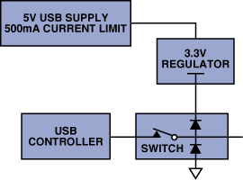
Figure 10. Switch in a normal USB situation with no stress.
图 11 显示了从 5 V 电源到数据线的短路(红色)。如果设备插入故障端口,就会出现这种情况。
| Figure 11 introduces a short (in red) from the 5-V supply to the data line. This could happen if the device were plugged into a faulty port. |

Figure 11. Positive supply of switch forward-biased.
短路会将 ESD(静电放电保护)二极管正向偏置到 VDD,这意味着 500 mA 电流会持续流过 ESD 二极管,这种情况可能会对 CMOS 开关造成极大的损害,因为它不可能存活超过 24 小时。这是实施 0.35 微米部件的一个限制。在需要满足这种 USB 条件的系统中,如果要使用 3 V 开关,设计人员需要提供足够的保护以防止这种故障机制。最简单的方法是使用电阻器限制电流。不过,最常见的解决方案是通过使用 5 V 电源供电的开关来完全避免这种情况。
| The short circuit forward-biases the ESD (electrostatic-discharge-protection) diode to VDD, which means that 500 mA could flow continuously through the ESD diode—a circumstance potentially very damaging to the CMOS switch, which would not be likely to survive over 24 hours. This is a limitation in implementing 0.35-µm parts. In systems that require this USB condition to be met, and a 3-V switch was to be used, the designer would need to provide adequate protection to prevent this failure mechanism. The easiest way of doing this is using a resistor to limit the current flow. However, the most common solution is to avoid this altogether by using a switch powered from 5-V supplies. |
Consumer Applications
在介绍了 USB 应用中使用开关的基本方法后,我们现在来考察一些特定的应用领域,并讨论它们使用开关的方法。我们将注意到,其中许多领域都有共同的拓扑结构。
| Having shown the basic ways in which switches are used in USB applications, we now survey some specific areas of application and discuss the ways they make use of switches. It will be noted that many of them have common topologies. |
Portable Media Players (PMPs)
PMP 正在迅速成为整个亚洲必备的小工具;据预测,它将很快取代 MP3 市场。PMP 可以直接从电视机、录像机、DVD 播放机、有线电视盒或卫星接收器录制节目,最多可存储 120 小时的视频、30 万张图片、16,500 首歌曲或 30 GB 的数据。能存储如此大量数据的便携设备必须具有快速、易用的接口。首选的接口通常是 USB 高速接口,可与 USB 摄像头、USB 读卡器或 USB 硬盘一起使用。
| PMPs are rapidly becoming a must-have gadget throughout Asia; it is predicted that they will soon replace the MP3 market. PMPs can record directly from a TV, VCR, DVD player, cable box, or a satellite receiver, and can store up to 120 hours of video, 300,000 pictures, 16,500 songs or 30 GB of data. A portable device that can store this amount of data must have a fast, easy-to-use interface. The interface of choice, usually USB Hi Speed, is one that can be used with a USB camera, USB card reader, or USB hard drives. |
消费者对这类产品的需求也决定了它必须是一款轻薄、便携的设备,因此传统笨重的耳机连接器根本不在考虑之列。取而代之的是一个迷你 USB 接口,USB 数据流和音频输出共用该接口。
| Consumer demand for this type of product also dictates a slim, portable device, so traditional bulky headphone connectors could not even be considered. Instead, the headphone connector is replaced by a mini USB connector, which is shared by the USB data stream and audio outputs. |
如图 12 所示,通常需要一个开关来隔离 USB 信号和模拟音频输出。在数据模式下,通过将音频信号与连接器 D- 和 D+ 引脚隔离,可最大限度地减少反射。快速信号逻辑状态转换期间的反射可能会导致更高的误码率,并违反 USB 高速连接的 500ppm 精度要求。
| As shown in Figure 12, a switch is typically needed to isolate the USB signal from the analog audio output. This minimizes reflections by isolating the audio signals from the connector D– and D+ pins when in data mode. Reflections during fast signal logic state transitions can potentially cause higher bit-error rates and violate the 500-ppm accuracy requirement of the USB High-Speed connection. |
对于此类应用,带宽宽、导通电阻匹配良好的开关有助于最大限度地减少 USB 信号边缘失真,而在音频模式下(输出连接到耳机),低导通电阻(约 2.5 欧姆)和低总谐波失真(约 0.1%)对于最大限度地减少音频失真至关重要。
| For applications of this kind, switches with wide bandwidth and good on-resistance matching help minimize USB signal-edge distortion, while in audio mode (output connected to a headphone), low on resistance (about 2.5 ohms), and low total harmonic distortion (about 0.1%) are critical to minimize audio distortion. |
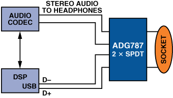
Figure 12. Sharing a mini USB connector between audio and USB.
Handsets/Cell Phones
随着手机功能的增加,设计者面临的挑战也随之增加。目前市面上的许多手机都有与个人电脑连接的电缆。这些连接用于传输数据,如电子邮件、日历、电话簿、闹钟、语音备忘录和计算器。如果手机集成了照相机,下载图片的功能也很有吸引力。
| As handsets acquire additional features, the challenges to a designer also increase. Many of the currently available handsets have cable connections to link to a PC. These connections are used to transfer data, such as emails, calendar, phone book, alarm clock, voice memos, and calculators. If the handset has an integrated camera, the ability to download pictures is also an attractive feature. |
因此,手机可能有许多功能需要兼容 USB 的开关。最常见的需求之一是在不同数据标准之间切换,例如在 UART 和 USB 之间切换。手机制造商希望保留为客户提供数据传输标准选择的能力,但他们无法承担为每个接口单独设计一个连接器所需的面积。最简单的解决方案是在一个通用连接器上复用多个引脚。图 13 显示了一个例子。
| So, a handset may have many features that generate a need for USB-compatible switches. One of the most common requirements is in switching between different data standards, for example, between UART and USB. Handset manufacturers like to retain the capability of offering a choice of data-transmission standards to their customers, but they cannot afford the area needed for a separate connector for each interface. The easiest solution is to multiplex a number of pins on a common connector. An example of this is shown in Figure 13. |
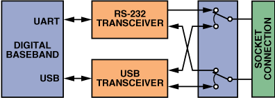
Figure 13. Switching between UART and USB using the switches on an ADG787.
高端手机设计中液晶面板显示屏和摄像头的分辨率不断提高,因此需要更大的存储设备,如嵌入式硬盘驱动器或外置小尺寸存储卡。大多数手机使用带有 USB 接口的独立硬盘控制器与 PC 主机通信。当基带处理器的全速 I/O 端口也用于同步地址簿或其他数据时,共享单个 USB 端口就成了一个难题。如图 14 所示,通过多路复用手机的 USB 连接可简化设计。
| Increasing resolutions of LCD panel displays and cameras in high-end phone designs generate a requirement for larger storage devices, such as embedded hard drives or external, reduced-size memory cards. Most cell phones use standalone hard-drive controllers with a USB interface to communicate with a PC host. When a full-speed I/O port for the baseband processor is also used for synchronizing address books or other data, sharing a single USB port becomes a challenge. The design is simplified by multiplexing the phone’s USB connection, as shown in the example of Figure 14. |
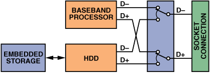
Figure 14. Multiplexing the USB port of a handset.
对于上述手机中的两种功能,设计者需要考虑的规格是:
* 是否符合所选 USB 标准的带宽要求?
* 导通电阻匹配和/或传播延迟匹配
* 低导通电阻平坦度/最小附加抖动
* 功率和封装尺寸。
手机的另一个功能是端口/总线隔离。这一功能不仅限于手机,还可用于其他便携式设计,如数码相机 (DSC)、PMP 和笔式驱动器。
| For both functions in a handset as described above, the specifications that need to be considered by the designer are: * does it meet the bandwidth requirements of the chosen USB standard? * on-resistance matching and/or matched propagation delays * low on-resistance flatness/minimal additive jitter * power and package size. A further function in a handset is port/bus isolation. This function, not limited to handsets, is also used in other portable designs such as digital still cameras (DSC), PMPs, and pen drives. |
开关通常用于保护可能受到外部噪声干扰的内部 ASIC。更重要的是:对于带有 USB OTG 接口的高端便携式设计,USB PHY(USB 物理层收发器)与外部世界之间的隔离可进一步降低在双功能设备(如两部手机)之间触发错误会话请求协议(SRP)脉冲的潜在风险。在这种应用中,开关选择的规格是断开隔离,当开关打开而 USB 端口未使用时需要断开隔离(图 15)。另一方面,当 USB 总线启动时,需要较宽的开关带宽,以实现最小的确定性抖动。Analog Devices 的许多开关都适合这种应用;本文末尾的表格是有用信息的主要来源。
| Switches are commonly used to protect internal ASICs that could be interfered with by external noise. Of greater importance: for high-end portable design with USB OTG interfaces, isolation between the USB PHY (USB physical layer transceivers) and the external world can further reduce the potential risk of triggering false session-request-protocol (SRP) pulses between dual-role devices—such as two cell phones. The specification of choice for a switch in this application is off-isolation, needed when the switch is open and the USB port is not in use (Figure 15). On the other hand, when the USB bus is activated, wide switch bandwidth is needed for minimal deterministic jitter. Many Analog Devices switches are suitable for this application; the tables at the end of this article are a compact source of useful information. |
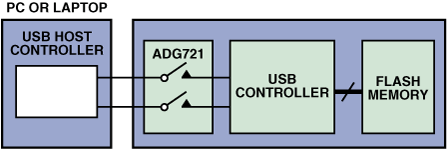
Figure 15. Dual-SPST switch used for isolation of USB.
Wireless Pen Drives and Wireless Adaptors
USB 闪存盘(笔式驱动器)因其移动性、无线功能和可扩展的内存大小,已成为办公室和家庭应用中数据共享的重要工具。另一种流行的设备是 USB 无线适配器;只需将其插入个人电脑,就可以无线连接互联网,而无需使用 Centrino™ 芯片。具有存储容量的 USB 无线适配器为商旅人士在无线互联网功能与存储和检索功能之间切换提供了方便。
| USB flash drives (pen drives) have become valuable tools for data sharing in both office and home applications because of their mobility, wireless capability, and scalable memory size. Another popular device is the USB wireless adapter; by simply plugging it into your PC, you can connect to the Internet wirelessly without the need for a Centrino™ chip, for example. Wireless USB adapters with memory storage capacity offer a convenient way for business travelers to switch between wireless Internet functions and storage and retrieval functions. |
大多数存储设备(如硬盘驱动器或紧凑型闪存控制器)都有高速 USB 接口,但没有集成到无线局域网 PHY 中。兼容 USB 的交换机可以在闪存存储和无线功能之间切换,从而轻松解决这一设计难题(图 16)。由于无线 USB 适配器的大部分功耗来自主机应用的总线,因此需要低功耗。小而薄的封装对于此类应用至关重要,因为笔式驱动器内部的印刷电路板空间非常有限。
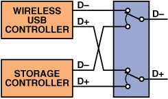
Figure 16. Using the ADG787 for memory/wireless switching in a USB wireless adaptor.
| Most storage devices such as hard-disk drives or compact flash memory controllers have Hi-Speed USB interfaces, which are not integrated into a wireless LAN PHY. A USB-compatible switch can easily solve this design challenge by switching between flash memory storage and wireless functions (Figure 16). Low power consumption is desirable, since most of the power consumed by wireless USB adapters comes from the bus of the host application. Small and thin packaging is critical for such applications with very limited PCB space available inside the pen drives. |
Personal Computers
电脑是大多数 USB 系统的枢纽。除 USB OTG 系统外,在所有其他系统中,个人电脑都是系统主机。许多传统的 USB 1.1 外围设备,如手机、数码相机、调制解调器、键盘、鼠标、某些 CD-ROM 驱动器、磁带和软驱、数码扫描仪和专用打印机,都与 PC 相互连接。现在,USB 2.0 高速接口可容纳全新一代的外围设备,包括基于 MPEG-2 视频的产品、数据手套和数字转换器。USB 已成为大多数个人电脑芯片组以及操作系统和其他系统软件的内置功能,而不会对个人电脑的价格产生重大影响。通过消除附加卡和独立电源,USB 可以使个人电脑外围设备的价格更加低廉。此外,USB 的热插拔功能使用户可以方便地安装和拆卸外围设备。
| The PC is at the hub of most USB systems. In all but USB OTG systems, the PC acts as the host of the system. The many traditional USB 1.1 peripherals, such as handsets, digital still cameras, modems, keyboards, mice, some CD-ROM drives, tape and floppy drives, digital scanners, and specialty printers—all interconnect with the PC. USB 2.0 Hi Speed now accommodates a whole new generation of peripherals, including MPEG-2 video-based products, data gloves, and digitizers. USB has become a built-in feature of most PC chipsets, as well as operating-system- and other system software, without significantly affecting PC prices. By eliminating add-in cards and separate power supplies, USB can help make PC peripheral devices more affordable than they would be otherwise. In addition, USB’s hot-swap capability allows users to easily attach and detach peripherals. |
与手机一样,CMOS 开关可用于在内部扩展 USB 总线。开关的另一个功能是外设复用。图 17 显示了多台 PC 共享一台打印机的情况。
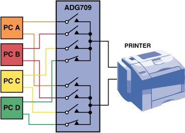
Figure 17. Connecting multiple PCs to a printer with an ADG709.
| As with handsets, CMOS switches can be used to expand the USB bus internally. A further function of switches is in peripheral multiplexing. Figure 17 shows a printer being shared by multiple PCs. |
Board Layout Considerations
信号布线是 USB 系统性能的关键。本节详细介绍了推荐的 USB 电路板信号布线。这些评论基于 USB-IF 选择的系统,目的是让电路板和电缆设计人员在设计电路板时尽可能减少对信号的影响。
| Signal routing is key to performance in USB systems. This section details recommended USB PCB signal routing. These comments are based on the system chosen by the USB-IF in order that board and cable designers could design boards that have as little effect. |
Authors 作者介绍
Padraig Fitzgerald 2002 年毕业于利默里克大学,获得电子工程学士学位。他于 2002 年进入爱尔兰利默里克的模拟器件公司,担任固态开关评估工程师,2007 年转入开关设计领域。Padraig 在科克理工学院完成了关于 MEMS 开关可靠性的硕士研究。他还获得了伦敦大学金融和经济学硕士学位。他目前是精密开关部门的首席设计工程师,也是 MEMS 开关的产品和设备设计师。
| Padraig Fitzgerald graduated from University of Limerick in 2002 with a bachelor’s degree in electronic engineering. He started at Analog Devices, Limerick, Ireland, as an evaluation engineer working on solid-state switches in 2002 and moved to switch design in 2007. Padraig completed a research master’s at Cork Institute of Technology on the reliability of MEMS switches. He also has a master’s degree in finance and economics from the University of London. He is currently a principal design engineer in the Precision Switch Group and is a product and device designer for the MEMS switch. |
参考:
Switching in USB Consumer Applications | Analog Devices
这篇关于USB - USB在消费领域的应用的文章就介绍到这儿,希望我们推荐的文章对编程师们有所帮助!